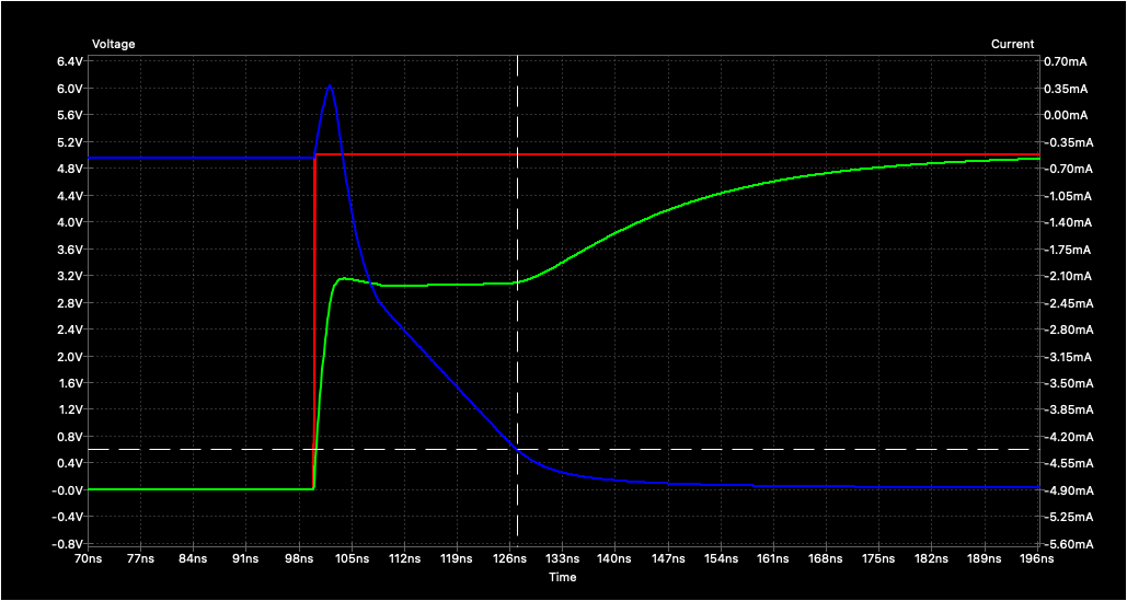
Last article we looked into the ramifications of using conductive ink PCB traces from a static, DC perspective. Today I'm going to consider the implications from a dynamic point of view. Most of the signal interfaces we use in microcontroller designs today drive very high impedance loads. The impact of increasing the trace resistance connecting to the input gate is an increase in the rise time. Let's take a look at that in more detail.
During this series, I plan to learn about printed ink conductors primarily on my own, through analysis and experiments. Therefore I have intentionally avoided digging too deep into the details of how they are commonly used in the industry (an approach I wouldn’t recommend for someone doing this for a professional product). But I do know people are indeed using printed inks for a variety of circuits, so I don’t expect to find any big showstoppers in the analyses and experiments that follow.
While repairing an old Ham radio transmitter back in high school, I found a bad capacitor. It was a large metal-can electrolytic type, bolted to the steel chassis of the radio. Because it was part of the negative 250 Vdc bias supply, the can was isolated from the chassis with an insulating fiber washer. Unfortunately, the replacement capacitor didn’t come with such a washer, and I couldn’t use the old one because it didn’t fit. Not to be deterred, I decided to make my own custom insulator using a piece of rubber cut from an old bicycle inner tube. To this day, I still remember the small explosion that resulted when I flipped on the power switch, not to mention the odor that was released – I dubbed it “Essence of Midnight in Pittsburgh”. I learned the hard way that inner tubes are not just rubber, but contain a substantial amount of carbon black and therefore don’t make very good insulators.
At NovaCentrix, we love working on projects that present real technical challenges with collaborators who think creatively and work smart. We have worked on many rewarding projects with both small research groups and individual researchers up to large multi-national technology companies. Working in printed electronics means exposure to many innovations – as the prints end up in an ever-growing number of devices (and it’s important to keep on top of process technology know-how). It can feel overwhelming to consider all the necessary details for creating a valuable and innovative new device, so I’m hoping that this post can help put us onto the path of success.
As a company, we bring many years of experience in printed electronics and a strong position in developing and understanding the latest techniques. I took some time to chat with one of our inks team experts (pictured) to talk about how an existing ink, or new ink, may be incorporated into a customer’s printing process. I’ve done so to build on the foundation laid by Rudy in his printing post, which I highly recommend reading [link]. I also recommend clicking through our Metalon Conductive Inks FAQ page which contains a lot of useful info [link].

Rudy Ghosh, our Technical Program Lead, was invited to wrap up the 2020 season of Tech Talk Thursdays for Global SMT International. It is super informative - and we hope you enjoy learning more about our high-intensity, pulsed-light solutions - and even a bit on NovaCentrix's history that you might not already know.

You might have seen on our website, tutorials and processes I’ve posted on how to embed electronics in garments. Too, I hope you’ll check out my YouTube clips included below.

Late fall in Austin is beautiful. Temperatures are in the mid-70s and it’s relatively dry – making it a great time to be outdoors. Combine the weather with Texans love for barbecuing and grilling, and eating outside with friends becomes a daily activity.
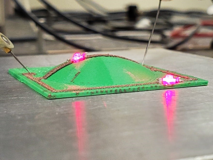
As a team, we love to highlight and share the work we see being done by researchers using NovaCentrix equipment and materials. While we regularly do this internally, my hope in sharing and writing about this recently published work for a broader audience is that it helps spread some interest in new tech, as well as bring attention to these great results. Researchers at the Army Research Laboratory and Duke University have shown that PulseForge curing can dramatically improve the electrical performance of 3D printed conductive filament composite materials.
3D printing, or additive manufacturing, has seen commercial efforts over several decades with a quick rise in interest over the past several years. A Gartner analysis from 2019 showed a 300% growth in enterprise 3D printer manufacturers over the preceding 3 years. Aerospace and medical device industries were among the first to create real value by using additive manufactur
ing to reduce weight and consolidate the assembly of components. Their success has paved the way for many other industries to evaluate new 3D printing techniques for their own processes.
Photonic curing is the high temperature processing of thin films using a flashlamp. When this processing is performed on a low temperature substrate, such as plastic or paper, a significantly higher temperature can be attained in the film versus an oven without damaging the substrate. This is due to two effects: 1) thermal processes exponentially progress with increasing temperature and 2 ) thermal damage to a polymer substrate generally takes a finite amount of time. Within a range, the shorter the time, the higher the temperature a material can take without damage. In the case of a polymer or paper
substrate, the ultimate temperature one can reach is right below its gasification temperature. The result is that an intense pulse of light can process a thin absorbing film on a low temperature substrate in only a few hundred microseconds as effectively or better than 10 minutes in an oven. As the substrate generally absorbs less of the light energy from the flashlamp than the targeted film, the film can be selectively printed and only the film is heated. That is, photonic curing is an automatically registering curing process. Consequently, even though photonic curing is very high in power, it is fundamentally a low energy process. Over the past 15 years, photonic curing has progressed far beyond the laboratory sintering of metal traces on plastic and paper and is now extensively used in many processes in the high-volume manufacturing (HVM) of consumer electronics.
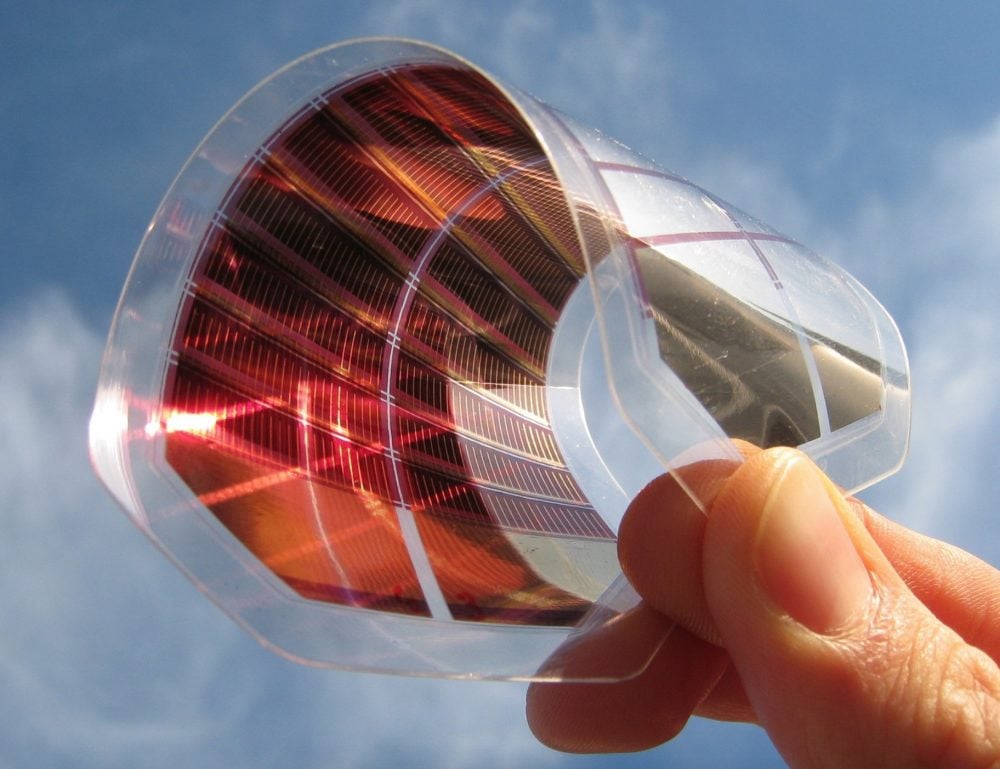
Perovskites are a group of organometallic/all-inorganic halides with chemical formula ABX3 in perovskite crystal structure1. Considered as a next-generation photovoltaic (PV) material, they combine strong light absorption with superior carrier transport2 and tunable bandgaps3.