

Perovskites are a group of organometallic/all-inorganic halides with chemical formula ABX3 in perovskite crystal structure1. Considered as a next-generation photovoltaic (PV) material, they combine strong light absorption with superior carrier transport2 and tunable bandgaps3.
Perovskite solar cells (PSC) are a fast-evolving PV technology since a landmark paper in 20094 by Kojima et al. The world record cell efficiency is now 25.2%5. Perovskite materials are made up of earth-abundant elements and inherently tailored to solution processability6, suitable for flexible substrates and ubiquitous PV applications.
The light absorbing nature of perovskites enables extensive use of photonic curing to fabricate and/or improve these materials. NovaCentrix has partnered with institutions around the world to better understand the properties of PSC and leverage the capabilities of PulseForge tools to enhance production of these devices. This document summarizes what has been found and next stages of developing this unique material system to revolutionize solar energy harvesting.
What practical challenges must be addressed in order to achieve commercial viability for PSC? How can photonic curing tackle those issues?
Key challenges:
- Stability: perovskite degradation can be induced by humidity, heat and irradation7,8
- Scalability: large-scale defect-free thin film deposition is yet to achieve9
These issues can be addressed by tailoring material properties, designing device structures as well as optimizing processing techniques. Photonic curing, as a power-intensive ultrafast photo-thermal technique, has the prospect for processing all the components in PSC.10–18
The transient nature (µs or ms scale) of photonic curing facilitates key advantages:
- For perovskite materials to achieve high temperature while circumventing thermal degradation
- For production to shorten processing time to less than millisecond scale combined with large-area capability
- For specific applications to comply with various flexible, temperature-sensitive substrates15
PulseForge systems have been applied to processing of different layers in the PSC fabrication. Here is a brief overview of the materials processed and outcomes:1. Photonic Curing of Photoactive (Perovskite) LayersPerovskites are generally deposited through a solution-processed pathway. To produce a smooth and compact layer, crystal growth is controlled through a complex step of rapid solvent removal9. Reported physical mechanisms to achieve supersaturation include anti-solvent extraction, gas-flow drying and in-situ heating9.Photonic curing carried out by PulseForge tools is an ultrafast thermal process equipped with unrivaled exposure uniformity (Figure 1), fine-tuned power intensity and temporal profile modulation. Integration of perovskite deposition and in-situ photonic curing allows efficient and controllable removal of solvents from perovskite layers.
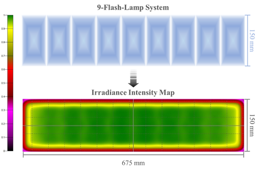
Figure 1. A 9-lamp beam intensity map displays extreme uniformity (±2% point-to-point) over a large area. PulseForge tools are modular and additional lamps can process a much larger area at similar uniformity.19
Additionally, photonic curing can be used for post-annealing to increase grain size and crystallinity of perovskite layer9. It has been investigated as an alternative to oven/hotplate heating. In both the planar (layer-by-layer) and mesoporous (TiO2 “sponge” soaked with perovskites) PSC structures, photonic curing was shown to form favorable morphology of perovskite layers, with no composition change or degradation11,13.
Photonic curing has also been applied in planar PSC13. After photonic curing, the perovskite morphology was shown to be greatly improved, i.e. larger grains and better surface coverage. Compared with reference PSC with the active layer heated at 70°C for 30 minutes, photonic curing improved the average efficiency from 8.21% to 11.5%.
Troughton et. al. directly applied photonic-cured perovskite layer in mesoporous PSC under ambient conditions11. The resulting power-conversion efficiency was comparable to that obtained with conventional hot-plate annealing. The two-step hot-plate annealing included 90-min heating at 100 °C followed by another 10 min at 120 °C conducted in a N2-filled glovebox, while the photonic curing process was done within a few milliseconds. In addition, the compatibility of photonic curing with ambient conditions alleviates significant practical barriers for industrial production in contrast to inert atmosphere annealing.
2. Photonic Curing of Transport Layers
TiO2 constructs the most common electron transport layer in PSC. It is spin-coated with or without binders, but high-temperature (~500 °C) annealing is always required to remove any organic additives and improve conductivity16. How does photonic curing improve the process?
TiO2 annealed at 500°C for 30 minutes in a furnace was compared with photonically cured samples with a pulse duration of 7 ms on glass substrate (2 ms for the PET substrate) by Das et al17. Comparable performance was shown (15.0% and 11.2% on glass and PET, respectively), but photonic curing enabled millisecond processing time and a significantly lower thermal input compared with furnace heating.
Similar studies have been conducted by multiple groups, where they photonically cured the TiO2 layer across various conditions and evaluated not only the efficiency but also the flexibility of their devices12,16. Comparable efficiency was found with conventionally annealed electron acceptor layers, demonstrating that photonic curing is an excellent alternative to provide efficient processing as well as compatibility with flexible substrates.
3. Photonic Curing of Electrodes and Encapsulation
Transparent conductive oxides and metals are conventional electrode materials for PSC. Carbon electrodes and solution-processed metallic ink are explored as alternatives as well8.
In a typical PSC structure, the metal electrode is the superstrate deposited on top of the temperature sensitive layers.9 During electrode fabrication, precise heating within the metal layer is required to avoid thermal degradation of the underlying device. This type of heating is achievable through photonic curing carried by PulseForge tools. Temperature profiles in the metal layer can be adjusted to meet specific production needs by tuning power density and pulse length.
Encapsulation20 is the last step to prevent PSC degradation, by insulating the perovskite layer from oxygen, moisture and/or heat. Common encapsulation materials are hydrophobic polymers. A functionalized fluoropolymer with luminescent down-shifting property was shown to improve device stability (under outdoor conditions for 2160 hours) as well as photocurrent generation (5% enhancement from the optimized composition)18. In this demonstration, the polymer precursors were cured under UV light to complete the cross-linking step. PulseForge tools can generate a broad spectrum of light with wavelength ranging from 200 nm to 1500 nm and shift the spectrum characteristics through intensity tuning, enabling efficient curing of such polymeric materials.
4. Intense Light Conditioning to Improving the Performance of a Completed PSC
Constant 1-sun illumination (power density of 100 mW/cm2) on PSC, i.e. light soaking, could induce both reversible and irreversible changes of perovskite composition, lattice parameters, defect migration, etc. Some of those changes could translate to better PSC performance. For instance, a tri-cation perovskite (FA0.7MA0.25Cs0.05PbI3) exhibited lattice expansion under light soaking, which mitigated interfacial energy barriers and simultaneously improved the open-circuit voltage as well as the fill factor21. A metal bi-halide perovskite (CsPbBrI2) underwent halide dealloying due to light soaking22, leading to significant improvement of hole conduction and thus power-conversion efficiency. These effects on perovskites can be reversed by dark condition, but irreversible changes were also observed in the electron transport layer, TiO223.
Whether photonic curing would lead to similar results on PSC performance in a shorter period of time, or whether the high peak power intensities (kW/cm2 scale) would bake in the favorable compositional/structural changes, are intriguing questions for future research. PulseForge offers powerful capabilities for fabrication of individual layers in PSC and have a promising outlook for processing of completed PSC to improve device performance.
Complete white paper and citations.