Late fall in Austin is beautiful. Temperatures are in the mid-70s and it’s relatively dry – making it a great time to be outdoors. Combine the weather with Texans love for barbecuing and grilling, and eating outside with friends becomes a daily activity.
One’s mastery of grilling perfect steaks, sausages and veggies is something we strive for here in Texas. And while a lot of grilling mastery comes from years of experience in knowing the right heat settings, types of wood to use, how long to wait, and when to move something from direct heat to less heated areas, even those of us with less experience can be successful… we just need the right tools.
One of my most trusted grilling tools is my non-contact IR thermometer. I point it at the different foods as they are grilling, and the temperature reading tells me when they are ready. And if I keep notes, I don’t necessarily need to repeat the temperature-check step every time. For example, I know that with my grill set at high heat, for a medium-rare steak, both sides need to cook for around 3-5 minutes.
If you have read this far, you might be asking yourself, when did this blog become a cooking blog? It hasn’t (yet). But a lot of the concepts of cooking on a grill are very similar to process development for most thermal procedures. Given these similarities, I’d like to lay out for you how in-situ visualization (similar to me using an IR thermometer during grilling) can help anyone become a Photonic Soldering Master!
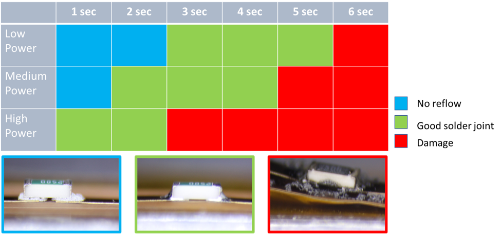
Since we are doing these measurements for process development of electronic components and thermal ramp rates that are very fast, I decided to switch my trusted grilling IR thermometer to something with a little more spatial and temporal resolution. For the process development matrix, we decided to track temperature changes as a function of average incident power density and exposure time, similar to what is shown in the first figure below. If needed, the digital controls on PulseForge tools allow us to make that window extremely granular – but it’s important to remember that the larger your process window, the easier your development path becomes.
Recorded directly from our IR camera, we shot videos to show how the temperature changes during soldering with PulseForge tools. For these demonstrations, we are using SAC305 solder to attach chip components (a resistor in 0603 package) onto a copper track with ENIG finish on a flexible polyimide substrate. For video1 (top), we chose a relatively low average power density and a long exposure time (3 seconds), while for video2 (bottom), we chose high average power density and a very short exposure time (0.75 seconds). Being able to measure the component temperature and correlating it to the input parameters allows us to target and reach peak temperatures consistently.
Below, we track the temperature changes as a function of average power densities for 1 second exposures. As expected, at higher average power densities, the temperature ramp rate becomes faster. This, in turn, equates to reaching reflow temperatures faster and can lead to a higher throughput. But the higher ramp rate also means small changes in processing time could lead to much higher peak temperature differences that could be detrimental to certain components or substrates (as well as the solder joints themselves).
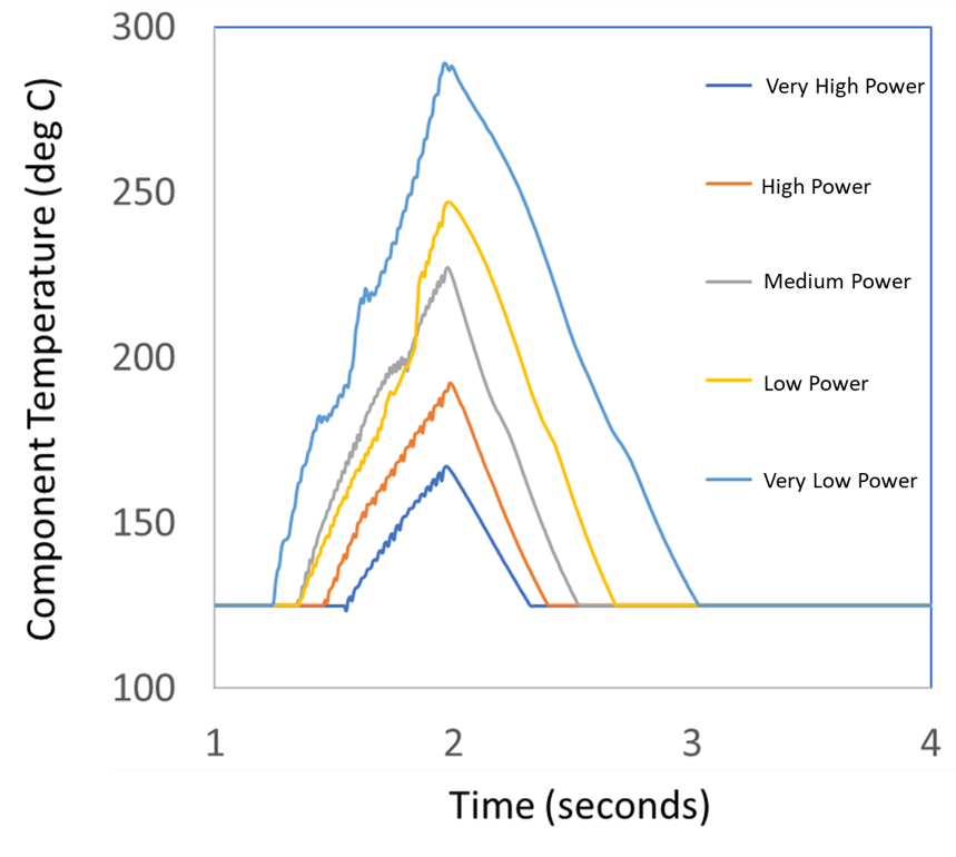
Another thing to note in the plot shown is that the cooling rate is very fast compared to conventional reflow processes. This happens because as soon as PulseForge light pulses are turned off, all energy sources are removed, and no residual heat remains behind. This fast cooling leads to very small granular microstructures, which correspond to high mechanical strength. But the fast cooling also leads to the structures more or less getting frozen in the state of the peak temperature reached. This ex-situ investigation of the solder joints lets us understand the process very clearly – even in the absence of high-end thermal cameras.
We will show results of that in a future blog. For now, it’s time to go back outside and enjoy the beautiful November weather in Austin.

Rudy is the VP of Business and Applications Development at NovaCentrix. Rudy joined NovaCentrix in 2017 and has since held roles ranging from Applications Engineer to Technical Lead and Director of Sales (at PulseForge). Currently, he focuses on business and applications development to align with NovaCentrix’s customer needs. Before NovaCentrix, Rudy was the Lead Scientist at Applied Novel Devices Inc., where he worked on ultra-thin solar cells for the Department of Defense. As a post-doctoral researcher at the University of Texas at Austin, he led efforts at the Microelectronics Research Center on 2D material growth. Rudy holds a PhD in Physics from the University of North Carolina at Chapel Hill and an MS in Physics from IIT Bombay. With over 20 years of materials science research experience and more than 30 technical publications, Rudy combines technical expertise and business acumen to support NovaCentrix’s customers.