
While repairing an old Ham radio transmitter back in high school, I found a bad capacitor. It was a large metal-can electrolytic type, bolted to the steel chassis of the radio. Because it was part of the negative 250 Vdc bias supply, the can was isolated from the chassis with an insulating fiber washer. Unfortunately, the replacement capacitor didn’t come with such a washer, and I couldn’t use the old one because it didn’t fit. Not to be deterred, I decided to make my own custom insulator using a piece of rubber cut from an old bicycle inner tube. To this day, I still remember the small explosion that resulted when I flipped on the power switch, not to mention the odor that was released – I dubbed it “Essence of Midnight in Pittsburgh”. I learned the hard way that inner tubes are not just rubber, but contain a substantial amount of carbon black and therefore don’t make very good insulators.
Despite my questionable background in less-than-perfect conductors, here at Chris’s Corner I’ll be covering this topic in a series of articles. The goal is to explore the use of conductive inks as printed circuit board (PCB) traces from an experimental point of view. I hope to shed some light on the various issues one must consider when using conductive inks in many common everyday circuits. After an overview of the technology, I will design and build a demonstration PCB where to simulate trace resistances electronically and evaluate the performance – how much resistance in a PCB trace can we tolerate? At the conclusion, I might build the same basic circuit board but using printed inks. Here is a rough outline of the series, but there could be some unexpected twists and turns along the way:
- Part 1: Introduction
- Part 2: Static DC Analysis
- Part 3: Dynamic AC Performance
- Part 4: Let’s Make a Reference PCB
- Part 5a: TraceR, 5b: Instrument Setup, 5c: MCU Test Board
- Part 6a: First Test Run, 6b: DC Performance Tests
- Part 7: Transient Analysis
- Part 8: Wrap Up, What’s Next?
What is Resistance?
Resistivity is an intrinsic property of a material. Don’t be confused when looking at data sheets. You’ll see this property variously called, Specific Resistance, Bulk Resistivity, Volume Resistivity, and/or Electrical Resistivity. Also note that the same material or element, such as copper, can have different resistivity depending on how it is prepared (such as annealed, drawn, pure, etc.). The same conductive ink formulation might have different resistivity depending on how it is applied and cured. Another effect is temperature – the resistance of many materials lowers with reduced temperature, and some materials become superconductors with zero resistance at extremely low temperatures. For the purposes of these articles, the term “material” will be used to indicate certain material + preparation + temperature combination.
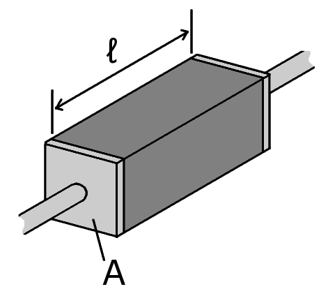
The basic definition of resistivity is the resistance per unit length of a material having a constant unit cross-sectional area. As the characteristics of PCB traces satisfy these conditions, this simplest definition will suffice. Resistivity is usually denoted by the symbol ⍴, and expressed in the SI units of ohm·meters (Ω·m). For most materials of interest, the Ω·m numbers are very small, like N✕10⁻⁸. In fact, having a resistivity around 10⁻⁸ Ω·m is the loose definition of a metal, and around 10⁺¹⁶ Ω·m an insulator. Because the values of resistivity are so small for metals, you’ll see it expressed in μΩ·cm.
I would have thought that units of conductance, mhos or siemens, would be used when talking about conductors and conductive inks. However, my initial review of data sheets suggests that speaking of their resistance is the norm. Therefore I’ll be using upside down ℧s (mhos) in keeping with the standard practice.
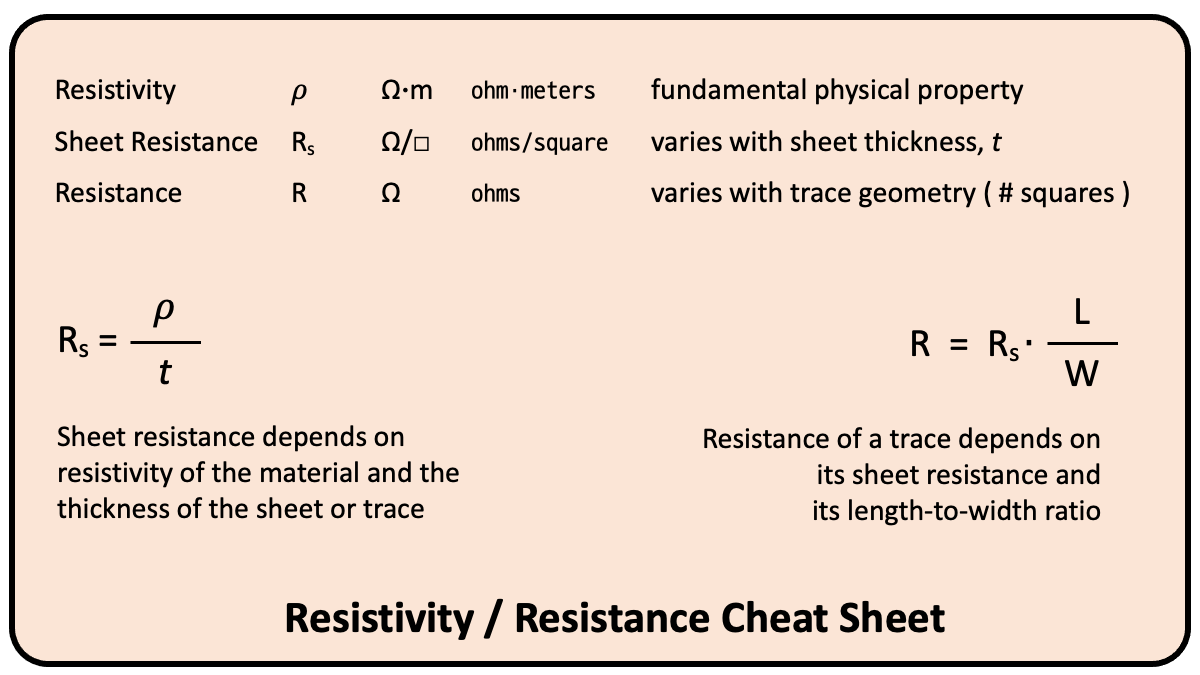
Sheet resistance, denoted by Rₛ, is expressed in Ω/□, where square is a unitless ratio denoting a square piece of material. Unintuitively, different sized squares of the same material will have the same resistance. Dave Jones has a good demonstration of this principle over on his EEVblog channel some years ago, where he measures various squares of conductive foam.
While resistivity may be useful in some circumstances, the sheet resistance of a material is more helpful when comparing thin strips of conductive materials such as PCB traces. This is especially so when different kinds of traces are applied in different thicknesses. Like resistivity, because of the small numbers involved sheet resistance is usually specified in mΩ/□.
Sometimes you may see sheet resistance of a material specified for a certain sheet thickness. For example, 190 mΩ/□ @ 1 mil. This caught me off-guard at first, because dimension-wise, this is equivalent to a resistivity ( 483 μΩ·cm ). Well, as it turns out, this is done as a computational convenience, since jumping around between Ω·m, μΩ·cm, Ω/□, and mΩ/□ can make your head spin. If we know a material has a sheet resistance of 190 mΩ/□ at 1 mil, it is easy to calculate its sheet resistance at, say, 2 mils ( 95mΩ/□ ) or at 1/2 mil ( 380 mΩ/□ ) by just dividing by the target thickness (you might also encounter sheet resistance normalized to one micron for similar reasons). Beware: this normalized sheet resistance may not be real – for example, it may not be possible to print a particular ink at 1 mil ( 25.4 μm ).
Summary:
- Resistivity: Ω·m or μΩ·cm– An intrinsic characteristic of a material
- Sheet Resistance: Ω/□ or mΩ/□– Describes a conceptual infinite sheet of uniform thickness and having uniform material properties throughout
- Resistance: Ω– The electrical resistance of a particular shape made out of one of these sheets
Copper – The Gold Standard of traces
Us engineers make a convenient simplification when designing circuits – the interconnections, like wires, PCB traces, and connectors, are usually considered to be perfect shorts. At least in the first-pass analysis. The experienced engineer knows when this doesn’t work, and will treat those cases differently. For example, the traces may need to be treated as…
- a series resistor in high current connections
- an RF transmission line for high-frequency signals
- a parasitic shunt capacitor in very high impedance circuits
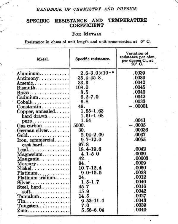
The foundation on which these assumptions stand is that the connection material, usually copper, has such a high conductance that it can be ignored in most circuits. Let’s quantify that. If we search online or dig out a dusty CRC Handbook, we find that the resistivity of copper is about 1.6 μΩ·cm.
Conductive inks
Conductive inks are designed to be conductive, but do not have the same properties as copper. Just how different are they?
First, there are four main conductive ink printing technologies:
- Silkscreen (think of tee-shirt or PCB lettering printing)
- Flexography (think of rubber stamps)
- Inkjet (think of your home color printer)
- Aerosol (think of an airbrush tee-shirt artist)
Basically these inks are all a mix of a base material, which is a binder (insulator), and conductive particles. Usually the conductive material is silver (Ag), but some inks use copper (Cu), cupric oxide (CuO), and even carbon ©. Selecting the exact ink and printing technology will be very specific to each project, considering the application, durability, flexibility, environmental factors, type of electronic circuitry, and many more. For my purposes, I’m going to conveniently ignore all these points and focus instead on the basic electrical properties.
Let’s take a more detailed look at those electrical properties. I reviewed 40-some inks listed on the Novacentrix website and collected their properties in one big table. Then I was able to group and plot their characteristics – a kind of conductivity competition. The goal is to see how the inks shape up against copper. To start off, let’s have a look at the resistivities of these various inks. And looking at this chart, it doesn’t look too bad for inks vs copper, yet.
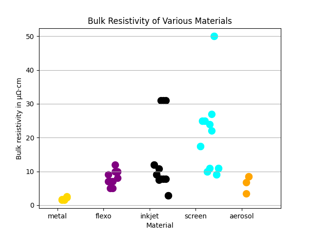
But to evaluate how they’ll work on a PCB, we have to consider how thickly the inks are usually applied. This next figure shows the range of typical thicknesses for each kind of ink. The four different copper thicknesses shown represent 1/2, 1, 2, and 4 ounce traces, corresponding to 17, 35, 70, and 140 μm, respectively. I’ll try to keep with the metric system and SI units, but in reality the PCB industry has one foot stuck in the imperial units camp and the other 0.3048 meters in the metric camp. This issue will come up again from time to time.
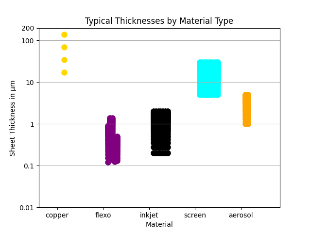
Now this is interesting. Judging by the resistivities alone, you might have given up on silkscreened inks. But considering they can be applied much thicker than other inks, they might be a good option after all. Now let’s calculate different sheet resistances for these inks, taking into account their usual thicknesses and range of resistivities.
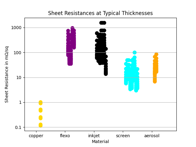
Well, it turns out silkscreened inks can get fairly close to copper. But as we expected, copper wins in all categories because its extremely low resistivity and that copper traces are much thicker than almost all inks.
There are a couple of reasons that conductive inks are deposited in much thinner layers than copper. Often an application using printed inks needs to be flexible, and thinner is better. The printing technique can also imposes some thickness limitations. And there is the cost to consider as well. The inks are more expensive than their copper counterparts. While they are usually made with silver, the processing required to make the inks drives their cost more than the precious metal content.
Typical PCB trace
In the next article I’ll look more at trace resistance and its effect on typical circuits. But let’s wrap up this introduction with a random signal trace on a typical PCB – say some kind of microcontroller. How about an 8 mil trace that runs 3 inches across a board made with 1 ounce copper (there are those pesky imperial units again). Let’s see what kind of resistance such a trace exhibits.
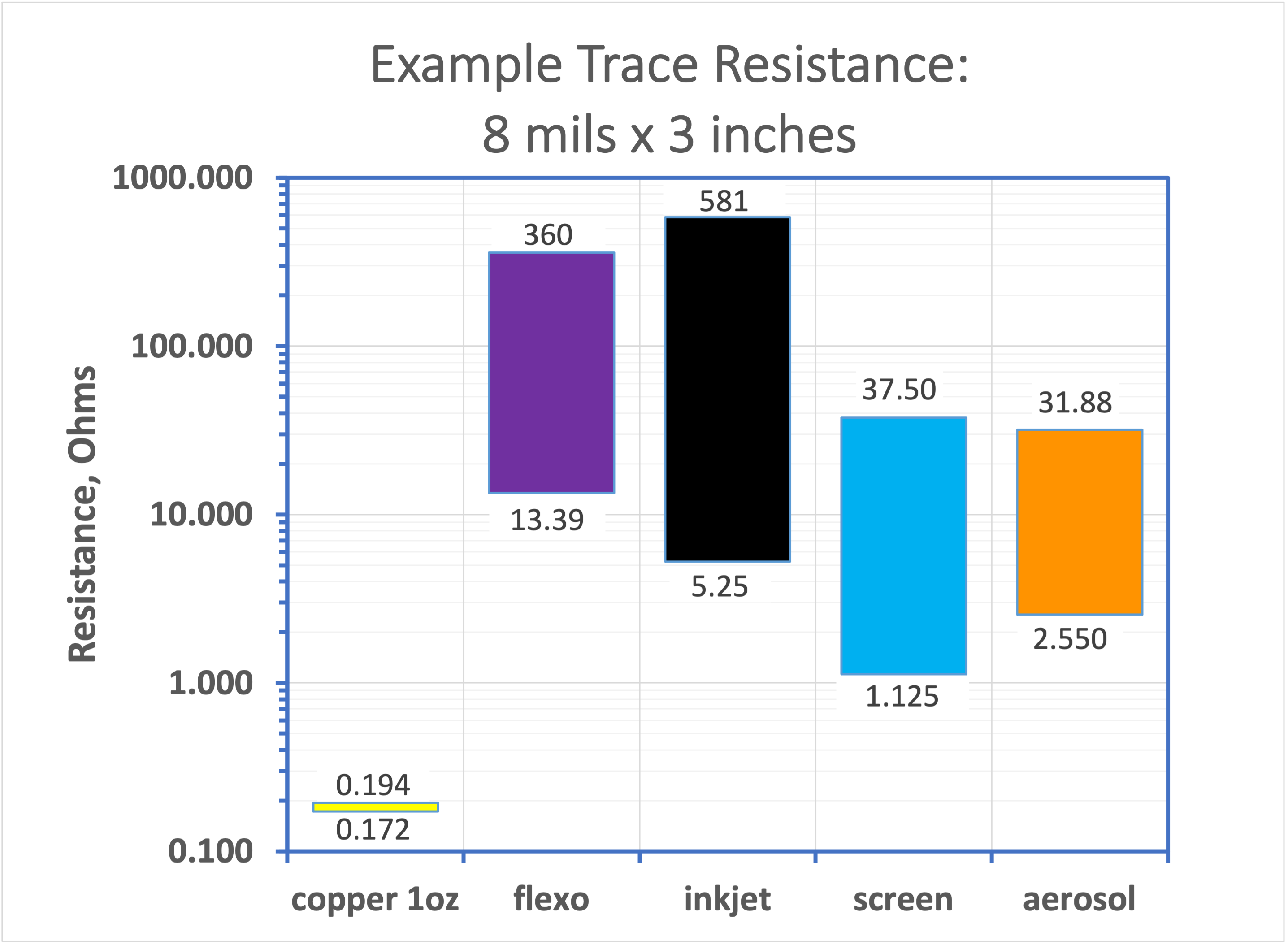
These results don’t look too bad. There would be some limitations using traces having hundreds of ohms in some circuits, but there are lot of options in the tens of ohms or less. This looks promising.
Part 2: Static DC analysis continues here.
Credits
- Resistivity geometry illustration from Wikimedia:
User:Omegatron, CC BY-SA 3.0, via Wikimedia Commons - Page 465, CRC Handbook of Chemistry and Physics, 8th Edition, 1920. from the Internet Archive, identifier ark:/13960/t2g751s54, Public Domain Mark 1.0
- Lead image: from NovaCentrix website