Late fall in Austin is beautiful. Temperatures are in the mid-70s and it’s relatively dry – making it a great time to be outdoors. Combine the weather with Texans love for barbecuing and grilling, and eating outside with friends becomes a daily activity.
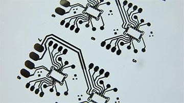
Photonic curing is the high temperature processing of thin films using a flashlamp. When this processing is performed on a low temperature substrate, such as plastic or paper, a significantly higher temperature can be attained in the film versus an oven without damaging the substrate. This is due to two effects: 1) thermal processes exponentially progress with increasing temperature and 2 ) thermal damage to a polymer substrate generally takes a finite amount of time. Within a range, the shorter the time, the higher the temperature a material can take without damage. In the case of a polymer or paper
substrate, the ultimate temperature one can reach is right below its gasification temperature. The result is that an intense pulse of light can process a thin absorbing film on a low temperature substrate in only a few hundred microseconds as effectively or better than 10 minutes in an oven. As the substrate generally absorbs less of the light energy from the flashlamp than the targeted film, the film can be selectively printed and only the film is heated. That is, photonic curing is an automatically registering curing process. Consequently, even though photonic curing is very high in power, it is fundamentally a low energy process. Over the past 15 years, photonic curing has progressed far beyond the laboratory sintering of metal traces on plastic and paper and is now extensively used in many processes in the high-volume manufacturing (HVM) of consumer electronics.