In the previous articles, we've taken a look at conductive ink PCB traces using a few back-of-the-envelope calculations. Now that we have a rough idea what to expect, it is time to get on with the fun part of this series -- building a real printed circuit board and testing how it behaves as we tweak the trace resistances.
Picking out MCU Design
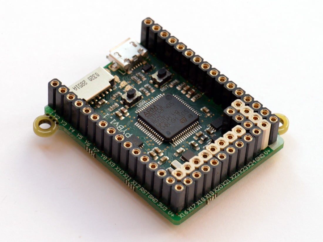
There are many basic Microcontroller Unit (MCU) board designs from which to choose. I want to select something that is commonly used, and have focused in on an ST Microelectronics Cortex M4 ARM MCU. Even this doesn't narrow down the options very much, as there are probably dozens of such board designs popular today. Since I plan to use Python and Micropython for controlling and collecting data from these experiments, I've decided to base our board's design on the standard Micropython pyboard. This board uses a very popular ST MCU, the STM32F405 variant. As with many modern Cortex families, this chip packs a bunch of powerful features, including:
- Cortex M4 with FPU
- 168 MHz
- 1 MB Flash Memory
- 192 KB SRAM
- A/D and D/A converters
- Serial I/O peripherals: USART, I2C, SPI, CAN
- USB, Ethernet MAC
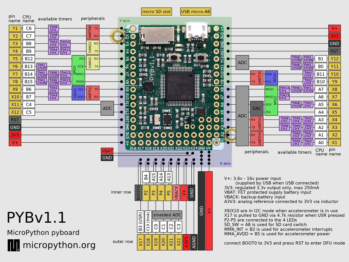
If you haven't seen the pyboard before, it is a compact, general-purpose embedded development board. Its design permits easy expansion, showcases the many of the features of the STM32F405, and acts as a good reference design for projects like ours.
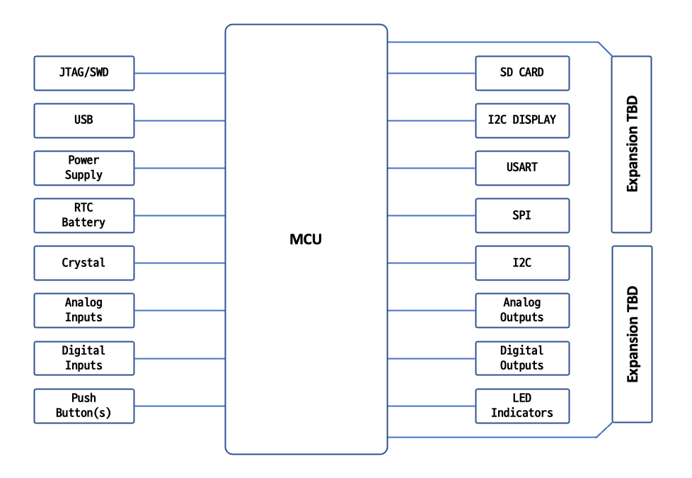
The purpose of this project is to experiment with trace resistance, our board doesn't need to be so compact. I'm planning to spread the components out, making the board a bit bigger. This will make it easier to probe around and take measurements. Also, I will add several dedicated peripherals onto the board rather than using the accessory expansion connectors like the original pyboard. However, I will put my own expansion connector to allow for testing of unexpected problems and/or interfaces if needed later on. Here is a block diagram which will serve as the starting point for the board (note that I haven't given it a name yet, just the generic Project MCU Board).
Testing Concept
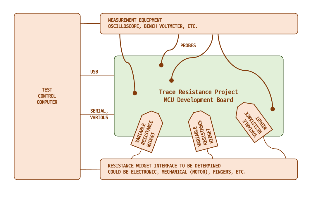
Let's use the example of serial communications using a basic UART to explain the testing concept. We establish a serial link between our MCU test board and a host -- which could be a desktop PC or a Raspberry Pi computer (more on this later). Known test data is sent back and forth over the link, and we look for errors as we crank up the trace resistance (more on this later, too). This notion is not unlike bit error rate testing, although the goal here is not really to measure bit error rates. Rather, it is find the trace resistance at which the communications link breaks down, and to determine why.
We could use a desktop PC for the above test, because they still have serial ports. Well, they don't actually have real serial ports, but almost all desktop PCs can easily communicate over serial links using USB-to-Serial adaptors. However, when it comes to other serial interfaces like I2C, SPI, CAN, etc., using a desktop PC can be awkward. An easier approach for these interfaces, and UARTs, is to use a Raspberry Pi computer. These have the functionality of desktop PC from the users point of view, regardless of whether you prefer GUI or the command line. And their hardware has built-in serial ports, I2C ports, and SPI ports which can easily be accessed by user programs.
Changing the Trace Resistance
You may be wondering, "How on Earth is Chris going to change the resistance of PCB copper traces?" Well, I'm not going to. Instead, I'm going to use a variable resistance on a trace to simulate increased trace resistance. This won't be perfect, of course, as the resistance will be lumped rather than distributed, as with conductive inks. But I still think useful results can be obtained with this approximation.
Now you are probably thinking, "This is going to be a huge board, with dozens of variable resistors installed on each trace." Well, not quite. Instead of putting so many variable resistors all over the board, I will put two-pin jumpers on most of the traces. This allows me to only install those variable resistors in the appropriate location as needed by the test at hand. The concept is best explained by this sketch:
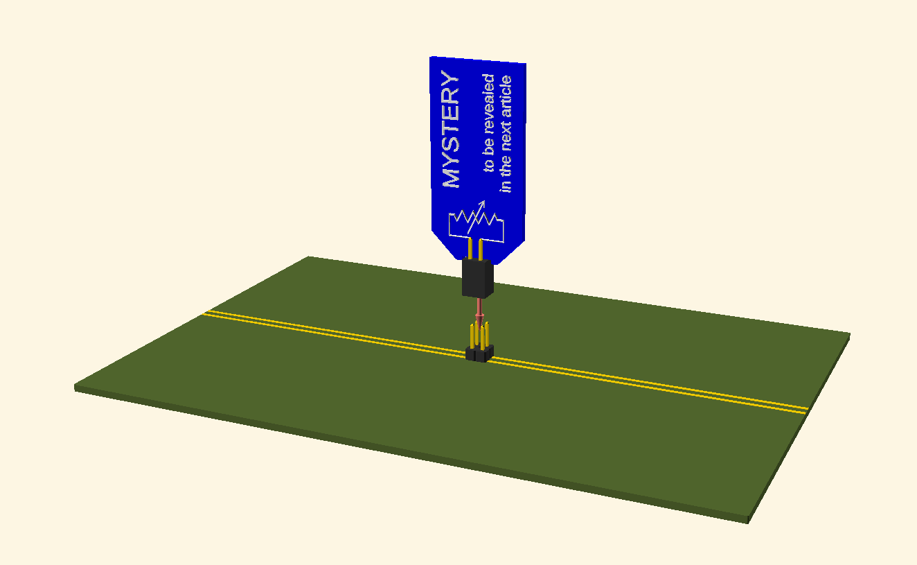
I'm holding back on the details of how I make this variable resistance until next article. But no matter the approach, having dozens of variable resistors on the board would indeed take up too much PCB real estate. By removing them from the board entirely, and going vertical as shown, it saves considerably on board space. A minimal penalty is imposed on the PCB design -- only a two-pin header on each signal that will be subject to trace resistance experimentation. And as an added bonus, we only need to make a few of these widgets, rather than one for every signal on the board.
What's Next?
The next article will describe the mysterious variable resistance device introduced above. Making a separate widget to simulate trace resistance wasn't expected when I planned the original series, but I think we can maintain the original order of the series by breaking up the next article into parts 5a and 5b. I'm also considering an unplanned article to go deeper into the details of the Project MCU Board design.
Continue to Part 5a.
Notes
-
Pyboard pinout from Micropython organization website: https://micropython.org/resources/pybv11-pinout.jpg
-
Pyboard photograph from Micropython organization website: https://store.micropython.org/product/PYBv1.1H