During this series, I plan to learn about printed ink conductors primarily on my own, through analysis and experiments. Therefore I have intentionally avoided digging too deep into the details of how they are commonly used in the industry (an approach I wouldn’t recommend for someone doing this for a professional product). But I do know people are indeed using printed inks for a variety of circuits, so I don’t expect to find any big showstoppers in the analyses and experiments that follow.
Although my focus is going to be on the electrical aspects of these inks, let’s take a very brief look at the different kinds of conductive ink printing technologies in use today.
Flexography
Flexography, or flexo, can print at high speeds and can print on very thin materials (adding a logo to a spool of packing tape, for example). There is a bit of setup involved, as printing plates must be made for each design, so flexo is better suited to high volume printing. The investment is pricey – a flexo printing setup can cost well over $100K.
Inkjet
This method uses the same concept as common inkjet printers, and in some cases an ordinary inkjet printer can be used with conductive inks. Inkjet printing, while not as fast as flexo, is very adaptable. There is almost zero penalty for changing setups from one design to another. Inkjet printing technology in tandem with optical inspection can also be used to repair broken traces on existing boards.
Screen printing
Screen printing has the advantage of an extremely low cost of entry and can be done by hand. With little effort you can be printing circuits on your kitchen table without breaking the bank.
Aerosol
Aerosol, as its name implies, atomizes the ink to deposit it onto a substrate. One advantage of aerosol printing is that it can apply circuits onto 3D objects, something that is almost impossible with the other techniques.
DC analyses
First of all, let’s have a look at some common types of circuits on a typical PCB and do a sanity check on the overall concept. But what constitutes a “typical” PCB? That’s a question which has no correct answer, but as the author, I get to pick one. And I choose something that is very common these days, a small microcontroller board with a handful of typical interfaces. There won’t be any Ku-band radars used in the design, nor will I be building a 480 Vac three-phase power supply. Voltages will be 5 Vdc or 3.3 Vdc, occasionally higher voltages up to 24 Vdc may be considered. I will want to use a crystal oscillator circuit to see how that performs. This gives a rough idea of the sample PCB I will be making for this project. The final details will be ironed out over the next couple of articles.
Kinds of interfaces
Power
Delivering power to a load, be it your on-board processing circuitry or an external sensor or actuator, is one obvious situation where the resistance of conductive inks could play an important factor. Let’s consider a few such circuits and see what happens.
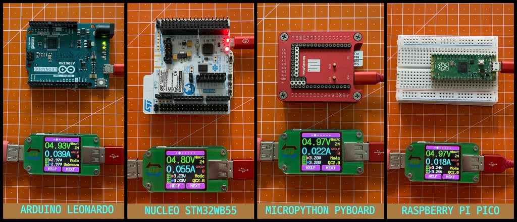
How about the power needs of a small microprocessor board? I took four random modules from my lab bench and measured their current draw. You can see from the result below that anywhere from say 20 mA to 60 mA was needed.
Using the arbitrary signal trace from the last article wouldn’t be fair. Even in a copper PCB, the power traces are generally thicker and shorter if at all possible. Let’s define an example power trace of 2 inches long and 25 mils wide. Running the numbers on this gives the following plot vs ink types.
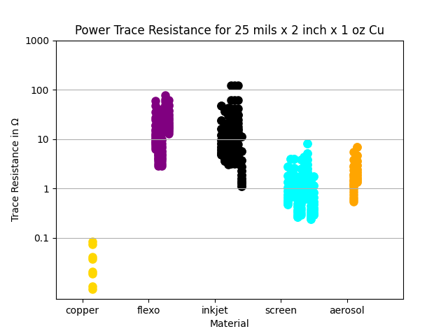
Looking at the plot, maybe 5 ohms is a good middle-ground that is achievable with all inks. Consider this simple schematic diagram showing the power traces as resistors.
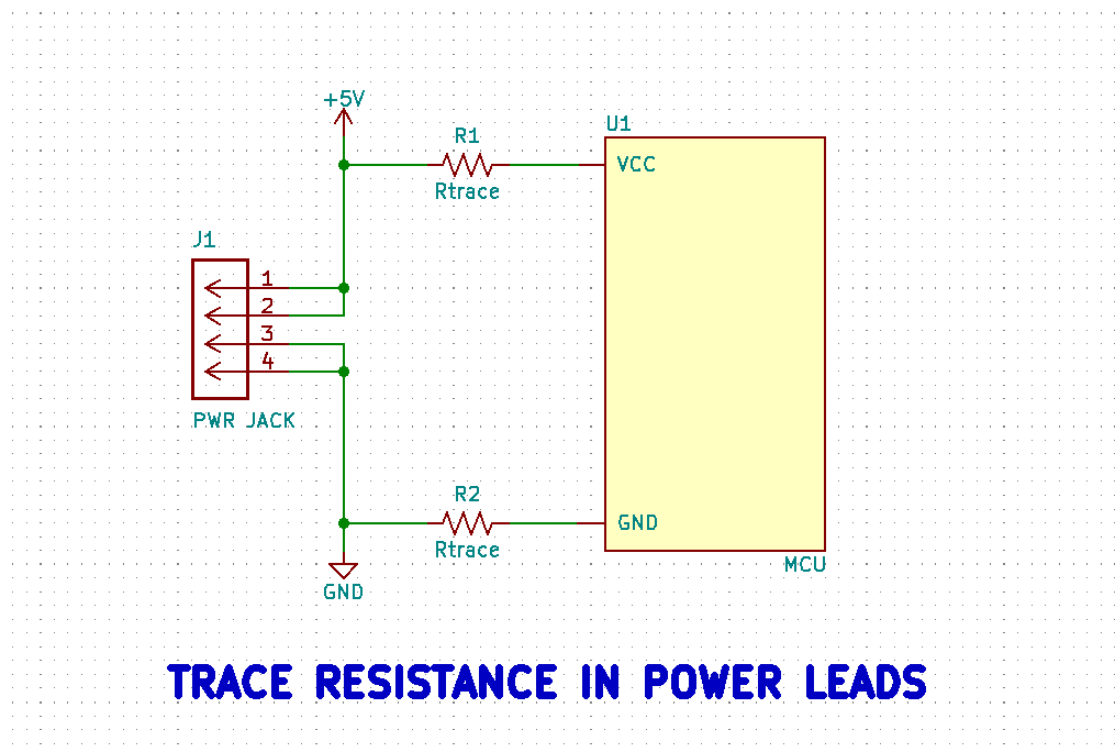
Let’s pick 100 mA of current being drawn from the power supply, the voltage drop across the power traces is 1/2 volt in each of the supply and return legs. I’m going to declare this as problematic. Distributing power is going to call for much wider traces. How about 100 mils (1/10 inch)?
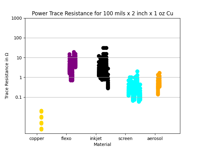
This is tolerable. At 100 mil trace width, a 1 Ω resistance is possible for all inks, and would present only 100 mV drop on each leg with a 100 mA load. This isn’t perfect, but it is something we can design around depending on the required current. Actual currents may be lower, and when needed, making wider traces shouldn’t be an issue. This does point out that a lot of care must be taken with return current management across the board. You don’t want different chips having different local ground potentials with respect to their neighbors. Or if it is unavoidable, at least we need to be aware of it and plan accordingly.
Signals
Compare to power, signals should pose little problems. Typical logic inputs on parts these days have very high input impedances, typically in the many MΩs. One very common shift register, the TI 74HC595, requires a maximum of only 100 nA input current. Signal traces resistances of few hundred ohms, as we calculated from the previous article (see below) won’t be an issue at all from the DC static perspective. I am concerned about the impact on switching speed, a topic to be addressed next article.
I/O Driving
What about higher current loads, such as LEDs, Relays, in the tens of milliamps? Having just run the numbers for power and signal traces, I’m going to wave my hands and declare “no problem”. Just put the driver circuit, a transistor, an RS-422 interface driver, etc., very close to the device or I/O connector. This way the higher current only flows a short distance and the trace resistance will be less important. This is something we usually do anyway when placing components on a PCB, so I am not seeing a big issue.
Wrap-up
After mulling over these numbers, I’m not worried yet. Power is going to be a challenge, signals less so. It occurs to me that the design and layout of a printed ink circuit board requires very close attention to current paths and returns. This is something we do (or should be doing) for ordinary copper PCB designs, but copper has such high conductivity that we can often get away with being lazy about current path management. I’m seeing that printed inks are not going to be as forgiving. But I’m excited – if I can learn to successfully design printed ink circuit boards, those skills will directly apply to ordinary PCB designs as well.
Next article I’ll do a little analysis of ink traces on the dynamic performance of a design. Intuitively I know that charging an input’s shunt capacitance is going to be slower through a resistive trace than copper. We’ll look at the numbers and decide whether that’s going be an issue or not. Then finally I’ll get around to building a PCB to demonstrate these concepts.
Tools
When calculating with numbers having the various units of Ω·m, μΩ·cm, Ω/□, mΩ/□, μm, cm, and mils, I really longed for my old HP-28 or HP-48 calculators. They could properly handle mixed-unit calculations. I installed an HP-48 emulator on my phone, but it wasn’t enough. I then discovered the Pint Python package. This package gives mixed-unit calculations to your Python script, or it can be invoked from the interpreter:
>>> import pint
>>> u = pint.UnitRegistry()
>>> th = 0.2 * u.microns
>>> sr = ( br / th ).to(u.milliohms)
>>> sr
<Quantity(450.0, 'milliohm')>
>>> sr.magnitude
450.0
>>> sr.units
<Unit('milliohm')>
>>>
In fact, several of the plots were prepared using Python. That code, along with a spreadsheet of various ink properties, is available in my GitHub repository. I will also be making additional repos for the experiments, PCB designs, etc., as the series gets rolling.
Part 3: Dynamic AC performance continues here
Credits
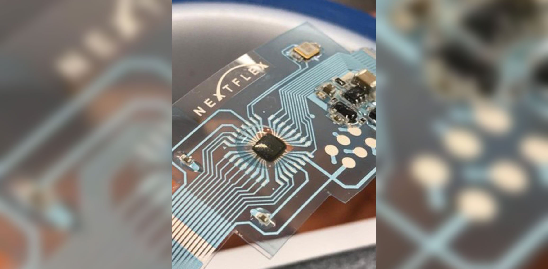
- Lead image: An Arduino built on flex PCB from NovaCentrix website
