

At NovaCentrix, we’re passionate about discovering how our products are advancing innovation through our customers and technical partners. Collaborations with academia are especially inspiring as they often push the boundaries of innovation, uncovering new possibilities for products and manufacturing. Today, we’re thrilled to spotlight groundbreaking research by Prof. Fernandez’s group at Norfolk State University. We had the opportunity to correspond with lead author of multiple publications in the area and a graduate student of the group, Harikrishnan Muraleedharan Jalajamony, to explore their use of atmospheric plasma-aided printing to drive next-generation flexible, stretchable, and wearable electronics applications.

Here are some highlights of the innovative work from Prof. Fernandez’s group that formed the basis of our conversation:
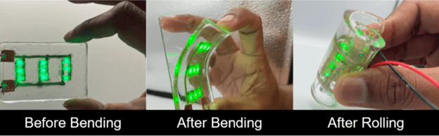
- Stretchable Electronics on PDMS: In their recent publication, “Plasma-aided direct printing of silver nanoparticle conductive structures on polydimethylsiloxane (PDMS) surfaces”, the group explored the use of silver nanoparticle conductive ink for creating stretchable electronics on PDMS. This work, published in Scientific Reports, showcases advancements in flexible electronics manufacturing and is available here.
- Triboelectric Nanogenerators (TENGs): The team extended their research to printing on silicone-coated fabric for TENG applications. This work, detailed in the Chemical Engineering Journal publication “Plasma jet printed AgNP electrodes for high-performance fabric TENGs and adaptive sensing applications”, demonstrates the technology’s potential in adaptive sensing. Access the paper here.
- Wi-Fi Antennas for Wearable Applications: At the IEEE SoutheastCon 2024 in Atlanta, the group presented “Plasma-Aided Inkjet Printing of Silver Nanoparticle Conductive Structures on PDMS for Wearable Applications”. This research highlights the method’s capability to fabricate Wi-Fi antennas for flexible and wearable devices. Read more here.
- NFC Antennas for Smart Masks: The development of NFC antennas for flexible, battery-less smart masks aimed at lung health monitoring was detailed in the IEEE FLEPS paper “Plasma Printed Antenna for Flexible Battery-Less Smart Mask for Lung Health Monitoring”. This cutting-edge application underscores the potential of plasma-aided printing for advanced wearable healthcare solutions. View the study here.
These groundbreaking studies illustrate the versatility and potential of plasma-aided printing in creating stretchable, durable electronics for wearables, sensors, and next-generation sensing systems.
Our questions to Hari are in blue and his answers are in black below:
How does atmospheric plasma-aided printing compare with traditional printing techniques (e.g., inkjet or aerosol jet printing) in terms of cost, scalability, and environmental impact for wearable electronics?
Atmospheric plasma-aided printing integrates surface modification and material deposition into a single process by combining the plasma plume with silver nanoparticle ink. As the plasma plume modifies the surface of the stretchable substrates such as polydimethylsiloxane (PDMS), creating temporary hydrophilic functional groups, the ink is simultaneously deposited, ensuring excellent adhesion and superior conductivity. This simultaneous surface treatment and printing eliminates the need for pre-treatment steps or high-temperature sintering typically required for hydrophobic substrates like PDMS [1]. The process is energy-efficient, environmentally friendly, and operates effectively at ambient temperatures, making it highly suitable for the scalable manufacturing of wearable electronics.
The scalability of plasma-aided printing is ensured by its straightforward setup, which does not require vacuum conditions or specialized thermal equipment. The plasma printer used in this study allows for adjustable parameters such as plasma voltage, print speed, ink mist rate, and gas flow rates. The system uses a precise ratio of wet gas (silver nanoparticle ink aerosol) to dry gas (inert gas of 95% argon and 5% hydrogen) to ensure uniform deposition and optimal activation of nanoparticles during the printing process. This combination ensures uniform nanoparticle deposition while maintaining the flexibility and stretchability of the substrate. The method also accommodates a variety of inks, in our research we used silver nanoparticle ink (NovaCentrix JS-A191), as well as other conductive and functional materials like copper, graphene, and metal oxides. These properties make plasma-aided printing particularly suitable for wearable electronics, which require flexible and stretchable components.
Beyond PDMS, this method’s versatility extends to printing on various substrates such as PET, polyimide, and even non-planar surfaces. PDMS, chosen in this study for its optical clarity, flexibility, and biocompatibility, was successfully patterned with conductive silver nanoparticle structures that maintained mechanical integrity under dynamic bending and stretching. These characteristics make the method ideal for wearable sweat sensors, smart textiles, and flexible circuits.
What challenges does this method address specifically for flexible and wearable electronics, and how does it enable new applications that were previously unattainable?
Plasma-aided printing addresses critical challenges in flexible and wearable electronics by enabling the creation of durable conductive structures on mechanically deformable substrates such as PDMS. The process forms a strong foundation layer by simultaneously modifying the PDMS surface with plasma and depositing silver nanoparticle ink. The plasma treatment creates temporary hydrophilic functional groups on the PDMS surface, allowing the silver nanoparticles to penetrate a few nanometers into its depth. This impregnation ensures exceptional adhesion between the conductive material and the substrate, providing a robust base for subsequent conductive layers. Without this foundation layer, the material would peel off due to insufficient penetration, making the formation of this layer essential for reliable stretchable electronics.
Successive plasma-aided printing of silver nanoparticles builds up a conductive layer with a thickness of ~1–7 micrometers. This multilayer structure maintains excellent adhesion and electrical conductivity, even under significant mechanical deformation such as bending, twisting, and stretching. The durability of these structures was demonstrated by their ability to retain performance after 1,000 cycles of mechanical stress, highlighting their suitability for real-world applications. The combined plasma treatment and deposition ensure that the conductive material not only adheres strongly to the PDMS surface but also delivers consistent electrical performance under dynamic conditions.
Additionally, post-print inert plasma treatment further enhances the conductive properties of the printed structures. Conducted under the same plasma conditions as printing but without feeding the ink, this treatment improves the surface characteristics of the conductive layer, ensuring better overall performance. Together, these steps—real-time plasma-assisted deposition and post-treatment—produce conductive structures with exceptional durability and reliability, making plasma-aided printing an ideal technology for advanced wearable applications like biosensors, health monitors, and adaptive textiles.
Can this process accommodate other conductive or functional materials (e.g., copper, graphene, or composites) beyond silver nanoparticles?
Yes, the atmospheric plasma-aided printing process can accommodate a wide variety of conductive and functional materials, making it highly versatile for flexible and wearable electronics. Plasma printing effectively deposits metals such as silver (Ag), copper (Cu), and gold (Au), as well as semiconductors and oxides like titanium dioxide (TiO₂), tin oxide (SnO₂), copper oxide (CuO), and zinc oxide (ZnO) and it is also capable of printing graphene. These materials can be deposited on a range of substrates, including paper, glass, polyimide, and polyethylene terephthalate (PET), showcasing the adaptability of this technique for diverse applications.
Your study demonstrates the effectiveness of plasma-aided printing on PDMS. Have you explored or do you anticipate success with other flexible substrates like PET or polyimide?
The study primarily focused on PDMS for its flexibility, biocompatibility, and suitability for wearable applications. We demonstrated the versatility of plasma-aided printing by fabricating Wi-Fi antennas on PET and polyimide substrates, showcasing its adaptability to various flexible materials. Additionally, our team successfully printed NFC antennas on flexible substrates for a battery-less smart mask application, further emphasizing the method’s potential for advanced battery-less wearable devices. Furthermore, we applied plasma jet printing to develop high-performance fabric electrodes for Triboelectric Nanogenerators (F-TENGs), achieving remarkable adhesion and durability while enabling efficient energy harvesting and real-time sensing applications. These advancements highlight the versatility and potential of plasma-aided printing for next-generation wearable technologies.
What modifications, if any, would be required to extend this technique to substrates with different thermal or mechanical properties?
To extend plasma-aided printing to substrates with different thermal or mechanical properties, modifications to plasma energy, exposure time, and ink formulation are crucial. For thermally stable substrates like polyimide, higher plasma energy or longer exposure can enhance surface activation, while heat-sensitive materials like PET or fabrics require reduced plasma intensity to avoid damage. Adjusting the printhead distance and ink misting rate ensures uniform deposition across smooth or porous surfaces. Additionally, tailoring ink viscosity and wettability to match the substrate’s surface energy improves adhesion and conductivity, enabling the method to be effectively applied to diverse flexible and wearable electronic applications.
Given the improvements in conductivity and adhesion, how does the process fare under real-world usage conditions such as repeated flexing, exposure to moisture, or temperature fluctuations?
Our work on PDMS using plasma-aided inkjet printing demonstrated that conductive patterns maintained excellent adhesion and conductivity even after 1,000 cycles of dynamic bending. This durability is achieved through the formation of a strong foundation layer during the integrated plasma treatment and printing process. The plasma jet modifies the PDMS surface in real-time, creating temporary hydrophilic functional groups and allowing the silver nanoparticle ink to penetrate a few nanometers into the substrate. This penetration forms a robust bond between the conductive material and the PDMS, ensuring exceptional adhesion and long-term durability.
By combining printing and plasma treatment in a single process, the method creates uniform and high-performance conductive structures that are ideal for wearable biosensors, smart textiles, and other flexible electronic applications. Additionally, encapsulation layers can be incorporated to enhance resistance to environmental factors such as moisture and temperature fluctuations, further extending the applicability of these structures in real-world conditions.
Are there specific wearable applications (e.g., biosensors, smart textiles) where you see this method making the most immediate impact?
The plasma-aided printing process is highly effective for smart wearables and textiles, particularly in fabricating conductive traces and antennas. Our team successfully demonstrated this by printing NFC antennas for a battery-less smart mask, Wi-Fi antennas on flexible substrates like polyimide and PDMS, and high-performance fabric electrodes for Triboelectric Nanogenerators (TENGs). These examples showcase the method’s ability to create durable and efficient wireless communication components and energy-harvesting devices directly on flexible substrates. This highlights the potential of plasma-aided printing to advance IoT-enabled wearable devices and adaptive textiles for a wide range of smart applications.
You identified 17 kV as the optimal plasma voltage for adhesion and conductivity. How precise does the voltage control need to be, and can this process be adapted for high-throughput manufacturing?
In this work, 17 kV was identified as the optimal plasma voltage for achieving excellent adhesion and conductivity of silver nanoparticle ink on PDMS. Precise voltage control is critical, as the required voltage varies depending on the substrate and ink properties. Achieving the right voltage is essential for forming a strong foundation layer, where the plasma modifies the substrate surface and allows the silver nanoparticles to penetrate a few nanometers deep, ensuring robust adhesion. Lower voltage conditions can result in weak plasma activation, causing the conductive structure to peel off due to an inadequate foundation layer. Conversely, excessively high voltage can damage the conductive structure by over-activating the substrate or nanoparticles, leading to non-uniform deposition or degradation of the printed layer.
Tailoring the voltage to the specific substrate and ink properties ensures uniform deposition, robust adhesion, and optimal conductivity, making the process versatile and reliable for flexible and wearable electronic applications. The identification of the optimal voltage, such as 17 kV in this study for silver nanoparticle ink on PDMS, underscores the importance of fine-tuning plasma conditions to achieve durable and high-performance conductive structures.
What are the potential bottlenecks in scaling up this technology for commercial production?
Scaling up plasma-aided printing technology for commercial production faces several potential bottlenecks. One significant challenge is maintaining uniformity over large substrate areas, as inconsistencies in plasma activation or ink deposition can compromise the quality and performance of the printed structures. Additionally, prolonged printing can lead to overheating of the print head, requiring periodic cooling to prevent performance degradation or equipment damage. The use of viscous inks poses another challenge, as they can clog the print head, necessitating regular maintenance and cleaning to ensure consistent operation. Addressing these technical issues is critical for achieving reliable, high-quality production at commercial scales.
Can this technique support multi-material or multi-layer printing for integrated circuits or complex wearable devices?
Yes, this technique can support multi-material and multi-layer printing. In our study titled “Plasma-aided direct printing of silver nanoparticle conductive structures on polydimethylsiloxane (PDMS) surfaces,” we successfully demonstrated multilayer printing to achieve a robust and highly conductive structure on PDMS. By building successive layers of silver nanoparticle ink using plasma-aided inkjet printing, we enhanced both adhesion and conductivity, ensuring the durability and performance of the printed structures under mechanical deformation.
Currently, we are further exploring the fabrication of flexible metal oxide and metal salt multilayers using plasma-aided inkjet printing, demonstrating the technique’s ability to support both multilayer and multi-material printing. This capability allows the deposition of multiple functional layers, each with distinct properties, enabling the development of advanced biosensors and other wearable electronics. By integrating different materials into the same structure, this approach provides the flexibility to tailor devices for specific applications, highlighting the versatility of plasma-aided printing in creating high-performance, adaptable electronic devices.
Are there opportunities for integrating functional layers, such as encapsulation or piezoelectric materials, using this method?
While we have not yet explored encapsulation or piezoelectric materials using plasma printing, it represents an intriguing opportunity for future work.
What industries or market segments do you see as the earliest adopters of this technology?
The earliest adopters of plasma-aided printing technology are likely to be industries focused on wearable electronics, biomedical devices, and IoT-enabled smart textiles. Applications such as flexible biosensors, adaptive smart clothing, and energy-harvesting devices are well-suited for this technology due to its ability to produce durable, high-performance, and stretchable conductive patterns on low temperature flexible and stretchable substrates.
Have you collaborated with any companies or organizations to prototype commercial applications, and what has been the feedback?
We have a research collaboration with the plasma printer inventers, Space Foundry Inc., where we developed a flexible NFC antenna for a battery-less smart mask as part of a National Science Foundation (NSF)-funded internship between Space Foundry and Norfolk State University (NSU). During this internship, a graduate student designed and fabricated the NFC antenna prior to the purchase of the plasma printing equipment. The results of this work were published at the IEEE FLEPS Conference held in Boston, USA in 2023, showcasing the potential of plasma-aided printing for flexible and wearable electronic applications.
Atmospheric plasma printing avoids high-temperature sintering. How does this contribute to the sustainability of the manufacturing process, particularly for wearables and disposable electronics?
Atmospheric plasma printing avoids high-temperature sintering, which significantly enhances the sustainability of the manufacturing process. By operating at ambient temperatures, this method reduces energy consumption and enables the use of low-temperature substrates, such as biodegradable materials like paper and cloth fabric. This not only minimizes the environmental impact but also supports the production of cost-effective and disposable electronics. Furthermore, the process is faster than traditional techniques, reducing the time required to develop conductive structures and making it an ideal solution for scalable and eco-friendly manufacturing in the wearables industry.
Are there additional steps in the process that could further reduce its environmental footprint?
Additional steps to reduce the environmental footprint of atmospheric plasma printing include using water-based or biodegradable inks to minimize chemical waste and exploring renewable or recyclable substrates, such as cellulose-based materials, paper, or fabric.
What are your next steps in refining this technology, and are there any ongoing projects exploring its use in novel applications?
Ongoing projects focus on developing multilayer printing for flexible biosensors and creating metal layers from metal salts, which can enhance the sensitivity and functionality of biosensors by improving conductivity and surface reactivity. We are also working on sensors using metal oxide nanoconjugate inks for bandgap-tunable applications, as well as developing biocompatible and low-cost sensors, such as pH and gas sensors, to expand the range of applications in healthcare and environmental monitoring.
Do you foresee integrating sensors, energy harvesting elements, or wireless communication components into the plasma-printed circuits?
Yes, we foresee integrating sensors, energy-harvesting elements, and wireless communication components into plasma-printed circuits. For instance, we successfully developed NFC antennas for a battery-less smart mask, integrating the SAMD21 low-power microcontroller and ST25DV16KV NFC chip to enable wireless communication and energy harvesting. Additionally, we have utilized plasma printing to coat silver nanoparticle layers on flexible silicone substrates for fabricating Triboelectric Nanogenerator (TENG) devices. These TENGs demonstrate efficient energy harvesting capabilities, paving the way for powering IoT-enabled wearable devices and advanced sensing systems.
How do you envision this process impacting the global printed electronics community, particularly in regions where manufacturing infrastructure may be limited?
This process can significantly impact the global printed electronics community by offering a scalable, low-cost solution that operates under ambient conditions without requiring high-temperature sintering or complex infrastructure. Its ability to produce high-quality conductive structures in significantly less time compared to traditional methods makes it particularly valuable for regions with limited manufacturing capabilities. This innovation enables the local production of advanced wearables and flexible electronics, reducing dependency on complex industrial setups and paving the way for accessible, efficient device fabrication worldwide.
Could this method democratize the production of wearables and flexible electronics, making them more accessible and affordable?
Yes, this method could democratize the production of wearable and flexible electronics, making them more accessible and affordable. While further research is needed, the faster fabrication process and compatibility with a wide range of inks and substrates, including PDMS, highlight its potential for scalable and cost-effective manufacturing. The successful use of plasma-aided printing on PDMS, a highly flexible and biocompatible material, demonstrates its suitability for creating advanced wearable devices, enabling broader adoption in diverse applications, even in resource-limited settings.
Thank you, Hari, for sharing your insights and taking the time to answer our questions. We’re excited to see how your work, along with the groundbreaking research from Prof. Fernandez’s lab, continues to push the boundaries of innovation in the rapidly evolving field of printed electronics. We look forward to following your future advancements!
References:
[1] Y. Kim, X. Ren, J. W. Kim, and H. Noh, ‘Direct inkjet printing of micro-scale silver electrodes on polydimethylsiloxane (PDMS) microchip’, Journal of Micromechanics and Microengineering, vol. 24, no. 11, p. 115010, Oct. 2014, doi: 10.1088/0960-1317/24/11/115010.