

Current Material Options
If you have ever disassembled any electronic device, you know that inside you’ll find a variety of components, such as resistors, capacitors, chips and controllers that make everything work. All of these components usually sit on a rigid board (with copper tracks on it) that allows these parts to talk to one another. A major consideration in the choice of materials for building conventional electronics is the material’s ability to withstand high temperature (a required step in building electronic devices). But if those high thermal requirements could be relaxed, it would open up a wide variety of material options which, in turn, would allow new forms and functionalities – while reducing unit costs.
Conventional Soldering and Reflow
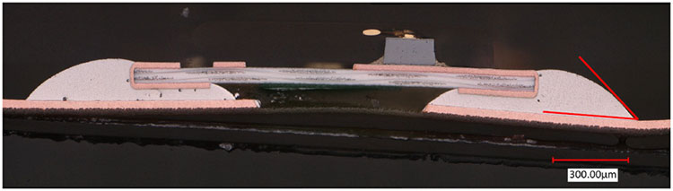
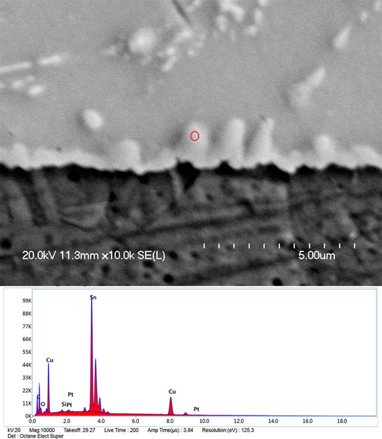
One of the processes that dictate the high thermal requirements of electronics is soldering. Conventional soldering processes depend on thermal processes that cause a metallic alloy to reflow and form strong joints between the pads of components and the conductive tracks. A good solder joint ensures reliability in structural strength, as well not losing communication between the different components that make up the electronic assembly. If we could ensure the advantages of conventional solder reflow processes without having to worry about the thermal process destroying our substrates, new forms of lightweight, stretchable, bendable, inexpensive yet reliable electronics could be produced. Selectively heating the solder using a laser beam is one way to go. However, with a focused laser beam, usually only a single joint is soldered at a time. With the increased number of components on every panel – where processing speeds are concerned – this can create a bottleneck
Enter Photonic Soldering
PulseForge tools used for photonic soldering employ white light over a broad area that allows whole panels to be processed within a couple of seconds.
PulseForge tools use high intensity, short duration (in the order of µs to ms) pulses of lights that allows fine tuning of thermal ramp rates, and thus have fine control over the material and structural properties of the final solder joints.
And the broad area light means solder reflow happens simultaneously at all terminals of the same component, which reduces soldering errors, such as tombstoning, while allowing alignment of components.
PulseForge photonic soldering tool models are suitable for R&D scale as well as SMEMA compliant assembly lines. Do you want to learn more about our technology and capabilities? Drop us a line at info@novacentrix.com.
One Response
Dear sir
Can Photonic soldering apply to the high density mounted components on the PCB? How to avoid the shadow effect?
Is the photonic soldering oven is available in the market now ?
We have a PCB with 5 pcs of IGBT module on one side , we need to solder the pins of those IGBT on the other Side of the PCB , Can the photonic soldering can apply to such application.
If possible , can you send the specification of the photonic soldering oven machine to me by email.
Thank you
Texas Sze
Email: texassze@ese.com.hk