

How Does the Photonic Curing Process Work?
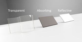 Light energy incident on a body will be absorbed and heat up the object. The light-matter interaction determines what fraction of light is reflected back, transmitted through or absorbed by the body. The fraction of light absorbed can be guessed by the color of the body (darker material absorbs more light). Light that is absorbed by the body is mostly converted to heat and shows up as an increase in its temperature. That’s why wearing a black shirt in the middle of a Texas summer isn’t the most comfortable thing to do.
Photonic curing processes use the same concept to heat objects up hundreds of degrees using pulses of high intensity light. Beyond simply making something hot, photonic curing gives a user tight control over how hot for how long. Depending on the light-matter interaction, a user can also selectively heat within a material stack if they wish. This degree of control is important for users who want to create controllable manufacturing processes.
Why do Metals and Plastics of the Same Color Behave Differently when Processed with the PulseForge?
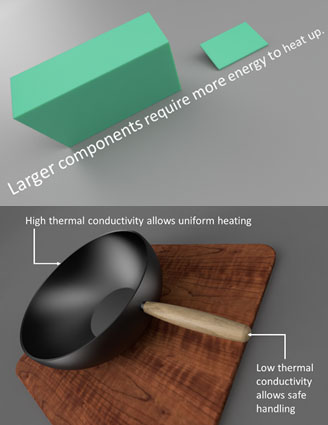 Once the absorbing body gets hot, it cools down by losing energy. The loss of energy happens in a few ways. It may go through some sort of phase transformation (by melting, changing its atomic crystal structure, etc.) or it may lose the heat to the neighboring bodies. How hot the body gets initially and how quickly it loses heat are dependent on its material properties (mass, heat capacity and thermal conductivity, respectively). Think about the difference between metal and wood and why metal cooking utensils often have wooden handles.
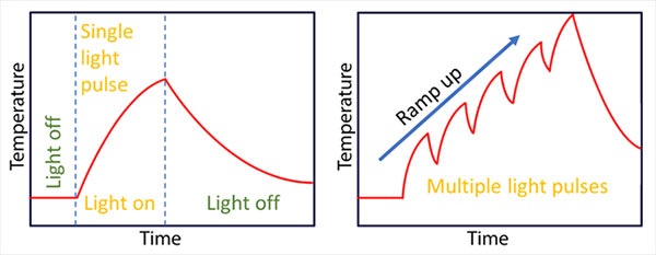
After a heating pulse of light, and given enough time, the heat loss from one body to another is complete, and both bodies will equilibrate to the same temperature. What happens if another pulse of light is applied before this equilibration temperature is reached? As more light is absorbed and converted to heat, the temperature of the body will start ramping up. How quickly this temperature rise happens is strongly dependent on the amount of light energy brought in per pulse, and how quickly each light pulse follows the last one. Once we can control and tailor the temperature gradient, we can use it for a variety of applications. An example application that uses this controlled ramp-up in temperature is photonic soldering.
How does Photonic Soldering Work?
 Before we get in to the details of photonic soldering, let’s see where soldering is required.
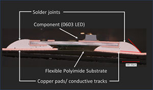
A very simple electrical circuit board consists of:
- substrate – conventional electronics regularly use FR4, but for flexible electronics this could be polymers such as polyimide, polyethylene or even fabrics
- conductive tracks – metallic tracks with or without protective layer (copper and silver are most commonly used)
- components – these could be passive elements such as resistors or capacitors, or components with built in logic that come in a variety of shapes, sizes and geometries, including number of terminals and their location
- solder/adhesives – these connect the components to the conductive tracks. The nature of the connections dictates the mechanical as well as electrical reliability of the whole circuit
Light hitting the circuit is absorbed at various positions. Thermal heating will be different on component, conductive tracks, exposed solder and the substrate. Depending on the component packaging (or lack of), the heat transfer to the solder can either be through the component or the terminal pads. Once the heat reaches the solder and gets it above a certain threshold temperature (called the liquidus temperature), reflow happens. Solder chemistry dictates that the reflowed material moves and wets higher temperature areas. Ideally, wetting happens at the metal terminals of the devices and various physical and chemical processes cause intermetallic layers and alloys to be formed.
The thickness (and chemical nature) of the intermetallic layer and the grain structure dictate the strength of the solder joint. These features can be controlled by how quickly (and how high) you can raise/ lower the temperature at the solder joint. As mentioned earlier, this controlled temperature ramp-up and ramp-down can be done using pulses of light.
Photonic Soldering with PulseForge Tools
With these PulseForge, short pulses of light can be modulated to control the ramp-up and ramp-down rates very precisely to tailor the material properties of the solder joints created.
The engineering aspect of photonic soldering is the ability to create thermal gradients for the most effective junction. And color differences between materials allows for an effective path to create thermal differences. Additionally, PulseForge soldering tools are designed to be able to do both top and bottom illumination. This enables the operator to apply the light in the direction most advantageous to the process.
What are the Advantages of PulseForge Soldering Compared to other Processes?
Instead of focusing on the details of every single soldering process (and there are many!), we can broadly categorize them into volumetric and selective processes. Conventional thermal processes, like a reflow oven, in which all parts inside the soldering chamber get to the same temperature, constitute a volumetric process. Laser soldering, which heats up only the solder joints, is a type of selective process.
Conventional thermal reflow processes are very mature and well understood. Most manufacturers have familiarity and access to the thermal reflow equipment and the expertise. However, the nature of the process itself is such that heating and cooling cycles are slow. As all parts get to the same temperature, the thermal stability of substrates, components, conductive tracks, coatings, etc., have to be pretty high.
To get around this limitation, selective heating with lasers is often used. However, laser processing is “too selective,” soldering a single joint at a time. And while each single joint can be soldered in ~one second, in highly dense panels, there could be thousands of individual joints that need to be soldered. This makes laser soldering a speed bottle-neck for high volume production.
Selectivity and High-Volume Processing
PulseForge soldering, which uses a broad-spectrum wide-area light source, has selectivity similar to lasers, while also having the capability of processing whole panels and boards within seconds. And because energy consumption happens only when the flashlamp is on (millisecond timescales), PulseForge photonic soldering is much more energy efficient than conventional thermal processes.
An added plus, the quick ramp-up and cool down that’s possible with PulseForge technology translates to a tool design with a footprint significantly less than conventional thermal reflow ovens.
Want to learn more about PulseForge tools and photonic soldering? Drop us a line at info@novacentrix.com
2 Responses
Please contact me regarding photonic soldering and curing. Thx.
Hello Chang,
We are looking micro soldering on micro pad and conductor wire on polyamide substrate. It can b possible with photonic soldering on low temperature (below 150 degree). I will share more details on it later on.
Kindly reply ASAP