Innovation in printed and flexible electronics thrives on collaboration. Across the industry, the most impactful breakthroughs happen when material scientists, process engineers, and system designers work together to solve complex challenges and bring bold ideas to life.
As part of our ongoing Partner Spotlight Series, we’re proud to feature our collaboration with Nanohmics, a Texas-based leader in advanced R&D and product development.
For over 20 years, Nanohmics has built a multidisciplinary team of scientists and engineers focused on applied materials science, micro- and nanofabrication, electro-optics, and embedded systems. Their work spans collaborations with U.S. federal agencies and industry leaders across defense, aerospace, biomedical, and energy sectors—delivering high-performance, field-ready technologies grounded in rigorous science.
To learn more about our collaboration and the innovation behind it, we spoke with Andrew Foley, PhD, Principal Scientist at Nanohmics. Our questions are in blue, followed by Dr. Foley’s insights in black.
Can you share the story of how Nanohmics got started and the initial challenges the company set out to solve?
Nanohmics was founded in 2002 by three scientists to transition innovative ideas, science, and engineering to develop early stage technology; specifically in the areas of novel materials, microfabrication, and instrumentation for electro-optic, sensors, power control, and other embedded systems/devices. We have been partnering with Novacentrix and Pulseforge for many years on materials and process development for a wide range of applications; including printed/flexible photonics. In 2019, Nanohmics began developing printed ferrites to improve safety communications infrastructure on highways, which eventually led to other application areas such as antenna miniaturization.
How did those early challenges naturally position you within the additive manufacturing and printed electronics industries?
The highway application led to multiple requirements on our materials and process from the get-go. The solution needed to be low-profile, high-volume, and low-cost so it could quickly scale to the hundreds of miles of smart corridors that the intelligent infrastructure industry is using as test beds before expanding to nation-wide deployment. The fabrication methods of the additive manufacturing and printed electronics industries were the perfect fit to address those problems. In hindsight, most industries prefer ready-to-scale and low-cost options when they are assessing new solutions.
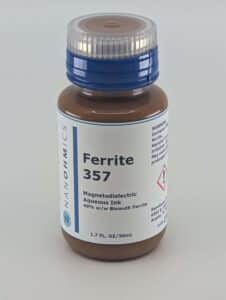
Our collaboration has centered on materials innovation, particularly Ferrite 357. What can you tell us about this material and the qualities that make it unique?
Ferrite 357 is a ceramic that can be cured on Kapton. Usually, the curing process for a ceramic would destroy any plastic substrate, but Ferrite 357 combined with PulseForge technology creates a way to rapidly cure that ceramic on a plastic without damaging that substrate. Ferrites are iron oxides, and they are both magnetic and dielectric. As a result, they shorten any magnetic or electric fields inside of them. Miniaturizing both types of fields at the same time makes them better for miniaturizing antennas than materials that are only dielectric.
The core material in Ferrite 357 is bismuth ferrite, which unlike many ferrites keeps its magnetic properties at the higher frequencies where WiFi operates. This high frequency performance makes Ferrite 357 great for making WiFi antennas smaller.
Which markets are showing the strongest interest in this technology right now?
We have seen the majority of interest from the RFID tag industry for miniaturization of printed tags using Ferrite 357. We have also had inquiries for developing alternate ferrites to act as RF shielding for computer hardware as well as ferrites for microwave circulators.
From your perspective, what makes the partnership between Nanohmics and NovaCentrix such a compelling collaboration?
Novacentrix’s technology already supports a mature printed electronics ecosystem, which is already well adapted for providing economical solutions to printed RF and microwave industries like RFID tags and printed antennas. Nanohmics’ printed ceramics, like Ferrite 357 and upcoming products, give that ecosystem a key differentiator from other fabrication methods; namely, ceramics that are readily inserted into existing fabrication streams for printed electronics. Beyond miniaturizing RFID tags and WiFi antennas, multiple microwave components like phase shifters, varactors, and circulators rely on ceramic materials to function. Our partnership opens up a simplified path to insert many of these materials-dependent components into the printed electronics industry.
Beyond Ferrite 357, what other material directions is Nanohmics currently exploring in the printed electronics and advanced materials space?
Nanohmics is developing various printed materials including other ferrites. These materials include ferroelectrics for beam steering components, piezoelectrics for strain sensors, lossy ferrites for microwave absorbers and RF shielding, and low-loss ferrites for microwave circulators.
We’d like to extend our sincere thanks to Dr. Andrew Foley and the entire Nanohmics team for sharing their insights and for their continued partnership. Collaborations like these are what make it possible to push the boundaries of what’s possible in printed and flexible electronics.
We’re excited about the work we’ve done together so far—and even more excited about what’s ahead.
Stay tuned for more partner highlights as we continue to showcase the incredible teams and technologies shaping the