
At NovaCentrix, we know that innovation in printed and flexible electronics isn’t just about having the best technology—it’s about building the right ecosystem. The real breakthroughs happen when companies collaborate across the value chain to turn great ideas into real-world solutions. That’s why partnerships are at the heart of everything we do.
In this spotlight, we’re excited to highlight our collaboration with Voltera, a leader in materials dispensing systems and printed electronics.
Voltera’s expertise in precision dispensing and rapid prototyping is a perfect match for our Metalon® conductive inks, making it easier than ever for engineers and researchers to bring their designs to life—from early-stage concepts to full-scale production.

To dive deeper, we caught up with Thomas Pol, Applications Lead at Voltera. Tom has been with Voltera for 5 years and works closely with customers to help solve their toughest applications and technology challenges. Our questions are in blue, and Tom’s responses are in black below.
Tell us a little bit about Voltera.
Founded in 2013, Voltera is a Canadian company that makes rapid prototyping platforms for printed electronics — from traditional circuit boards to flexible, stretchable, conformable, and biocompatible electronics of tomorrow.
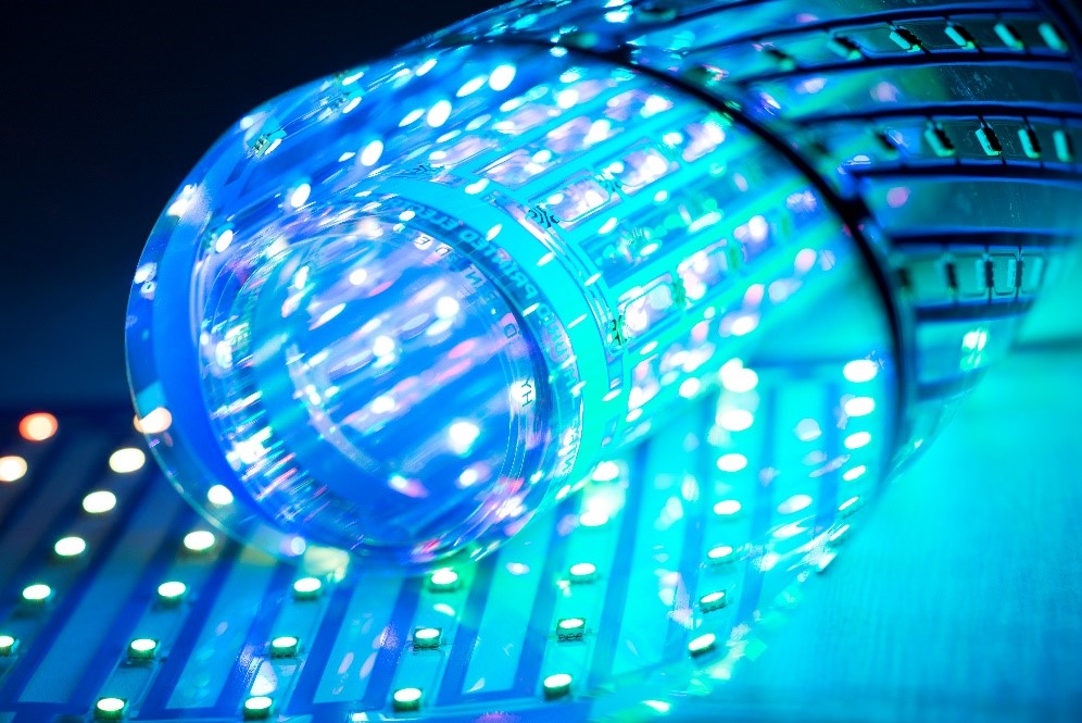
Our materials dispensing system, NOVA, is built for printing flexible hybrid electronics. It can dispense screen printable materials on flexible, stretchable, conformable, and biocompatible substrates, as well as rigid substrates like FR1, FR4, silicon wafers, and more. It is an ideal tool for:
-
- Flexible hybrid electronics R&D
- Precise material dispensing
- Novel materials research
- Seamless transition from testing to mass production
We also make a desktop PCB printer, V-One, which can drill through-holes, print conductive traces, dispense solder paste, and reflow on its heated bed — making it an excellent solution for in-house electronics R&D.
With thousands of customers worldwide and hundreds of mentions in published research, we are well on our way to achieving our mission: Catalyzing innovation by removing barriers to entry in the printed electronics industry.
What is the dispensing technology that is used by the V-One and the NOVA? How is it different from conventional processes such as screen printing?
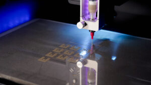
Both V-One and NOVA utilize direct-ink-writing (DIW) technology, an extrusion-based additive manufacturing process that deposits conductive inks, solder pastes, and other functional materials onto substrates feature by feature through a nozzle.
Compared with screen printing, Voltera’s products offer several advantages:
| Criteria | NOVA and V-One | Screen printing |
| Tooling required | No tooling required | Requires custom stencils or screens for each design, significantly increasing costs for small batches |
| Rapid iteration | Yes. Users can test a material or create a prototype in less than an hour. | No. Time-consuming and costly stencil changes are required. |
| Material waste | Precise control over material deposition, minimizing waste | High material waste due to excess ink usage and stencil cleaning |
| Ease of use | Easy to use, with intuitive software | Requires experience and manual setup |
| Accessibility | Accessible to both novices and experts | Requires intensive training to get started |
In addition, NOVA is equipped with a smart dispenser and a high-resolution camera, offering distinct advantages over screen printing in several key aspects, while maintaining comparable performance in print thickness and alignment accuracy:
| Criteria | NOVA | Screen printing |
| Trace width | A minimum trace width of 0.1 mm, with no added cost, providing high precision and allowing for the creation of fine, detailed features | Trace widths narrower than 5 mils (0.127 mm) will increase the cost significantly |
| Layer count | 4 stackup layers; multiple materials can be assigned to each layer | Typically limited to 2 layers, more layers require complex setup |
| Compatible materials | About the same as screen printing. It supports most screen-printable materials, including conductive inks, composites, epoxies, encapsulants, and custom inks. | Supports a wide range of inks, pastes, and adhesives |
| Alignment accuracy | Camera assisted alignment, with a 17 µm/px camera resolution, about the same as screen printing | Manual or semi-automatic alignment, accuracy varies |
| Print thickness | About the same as screen printing and dependant on ink viscosity | 10 – 20 µm per layer |
What are the biggest advantages of the NOVA and V-One? What specific customer pain points do they solve?
The biggest pain point NOVA solves is the lack of an efficient, high-precision, and versatile solution for prototyping additive electronics using screen-printable materials — a challenge that existing technologies like screen printing, inkjet printing, and alternative dispensing systems fail to address effectively.
Traditional screen printing, while dominant in additive electronics manufacturing, is not conducive to low-volume, high-precision prototyping or materials research due to costly and time-consuming tooling, excessive material waste, and the inability to easily iterate designs.
Inkjet printing offers digital flexibility but is limited by the narrow range of compatible materials, challenges with substrate compatibility, and the need for extensive expertise to optimize printing parameters. The high solvent content in inkjet materials also causes lower functional performance and poor scalability for production.

Compared to other DIW systems, NOVA stands out by offering an intuitive, user-friendly experience tailored for screen-printable materials. Competing systems often present significant usability issues, requiring manual calibration, extensive setup, and frequent maintenance, which can pose challenges to productivity.
NOVA addresses these challenges by providing a high-precision, modular dispensing platform that:
- Eliminates tooling costs and delays, enabling rapid iteration with on-the-fly design changes without additional expenses.
- Delivers precision dispensing, achieving minimum feature sizes down to 0.1 mm with tight control over material flow and deposition.
- Minimizes material waste, dispensing only where needed and containing materials throughout the process to reduce cleanup and handling risks.
- Ensures seamless compatibility with screen-printable materials, allowing users to transition from lab to production effortlessly.
- Simplifies the user experience, with intuitive software, guided workflows, and minimal setup requirements.
As such, NOVA empowers users to accelerate their research process or product development cycles while significantly reducing long-term costs.
V-One
The biggest pain point that the Voltera V-One solves is the time-consuming and costly process of prototyping PCBs using traditional methods such as PCB factories and isolation routing CNC machines.
In terms of technology and market space, where do you see the biggest pull from?
NOVA serves a broad range of industries, including healthcare, flexible hybrid electronics, aerospace, automotive, and industrial manufacturing, catering to both industry and academia.
Corporate R&D teams and contract manufacturers utilize NOVA to accelerate electronics product development and streamline the transition from lab to production. Material manufacturers leverage it to prototype and validate new materials, while academic institutions adopt NOVA for advanced materials and electronics research.
V-One primarily serves the PCB development and education sectors, including universities, high schools, fab labs, and product development teams.
Let’s talk a little bit about the materials that are used. What are you looking for as a material that is compatible with the NOVA?
In order to determine if a material is compatible with NOVA, we typically consider the following factors:
- Resistivity: Depends on the application; no specific value is required.
- Rheology:
- Viscosity should be within the range of 1,000 — 1,000,000 cps
- Reasonable recovery time — the more quickly the material stops flowing after shear stress the better it is for leakage prevention.
- Particle size: Typically under 25 microns to ensure consistent deposition.
- Slump: Dependent on both the material and the substrate properties. Ideally under 20% of the total printed width; less is preferable.
- Chemical composition: The ink should be safe to handle and compatible with the fluoroelastomer membranes used in our pressure sensor.
- Adhesion: The ink should be able to adhere to the substrate.
- Solderability: The ink should support the creation of strong, reliable solder joints.
How does NovaCentrix’s inks meet those requirements? What are the advantages?
Take the NovaCentrix HPS-U11 Silver Ink as an example. It offers several key advantages:
- Low slump: The ink retains its shape after deposition with minimal spreading, ensuring clean, well-defined prints and making it easy to use in precision applications.
- Excellent solderability and adhesion: It provides strong mechanical and electrical connections to various substrates, enhancing durability and reliability.
- Good resistivity values: With a resistivity range of 4.2×10⁻⁶ to 5.1×10⁻⁵ ohm-cm, the ink ensures efficient conductivity, making it ideal for high-performance electronic applications.
- Fine particle size: The small particle size allows the ink to be dispensed through smaller nozzles, enabling high-resolution printing without clogging issues.
- High viscosity: Its thick consistency minimizes leakage, ensuring precise deposition and reducing material waste.
Can you please elaborate on the partnership between Voltera and NovaCentrix?
We have a longstanding partnership with NovaCentrix, collaborating with them since the early days of our company. They offer a wide range of materials, and we continuously test their inks to assess their compatibility with our dispensing systems.
For example, NovaCentrix HPR-059 Carbon Ink works well with NOVA, and we now sell it on our store. Additionally, we have hosted a webinar featuring NovaCentrix inks — Printing Electronics with Carbon Ink using NOVA — and we look forward to organizing more webinars like this in the future.
“Our longstanding partnership with NovaCentrix is just the beginning. We are continuously exploring new opportunities to expand our material offerings, enhance compatibility, and unlock greater possibilities for our customers”.
Our collaborations with NovaCentrix mean more validated materials, seamless workflows, and increased confidence in achieving high-quality results — allowing users to focus on pushing the boundaries of innovation without limitations.