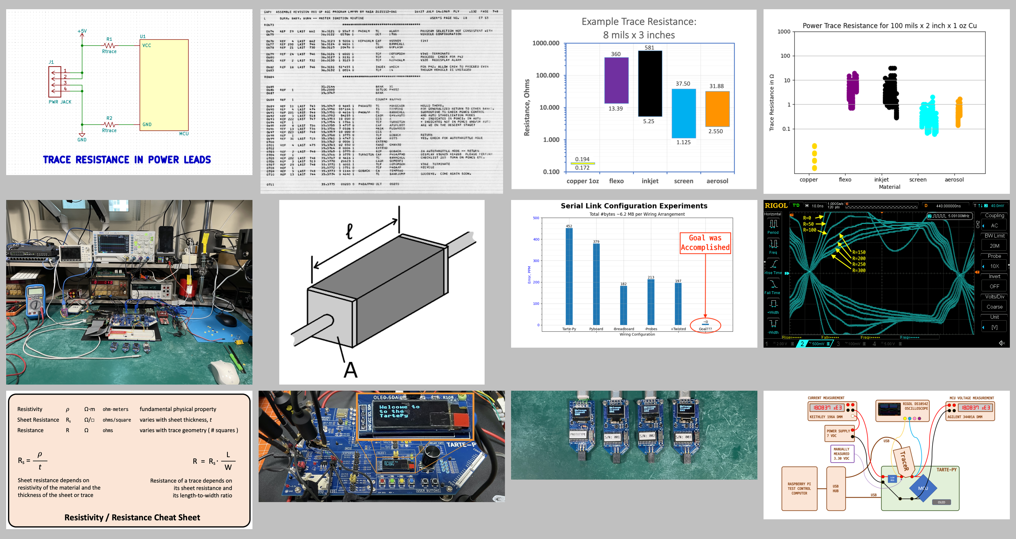
This is the final article of the series on conductive ink experiments. Let’s review the highlights of what we’ve learned, and summarize how we might use those lessons in a flexible circuit board design.
Resistance Fundamentals
We covered the basic property of electrical resistance in Part 1 of this series. I discussed the different kinds of conductive inks and how their properties differ from the “gold standard” of the PCB industry, the copper trace.
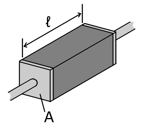
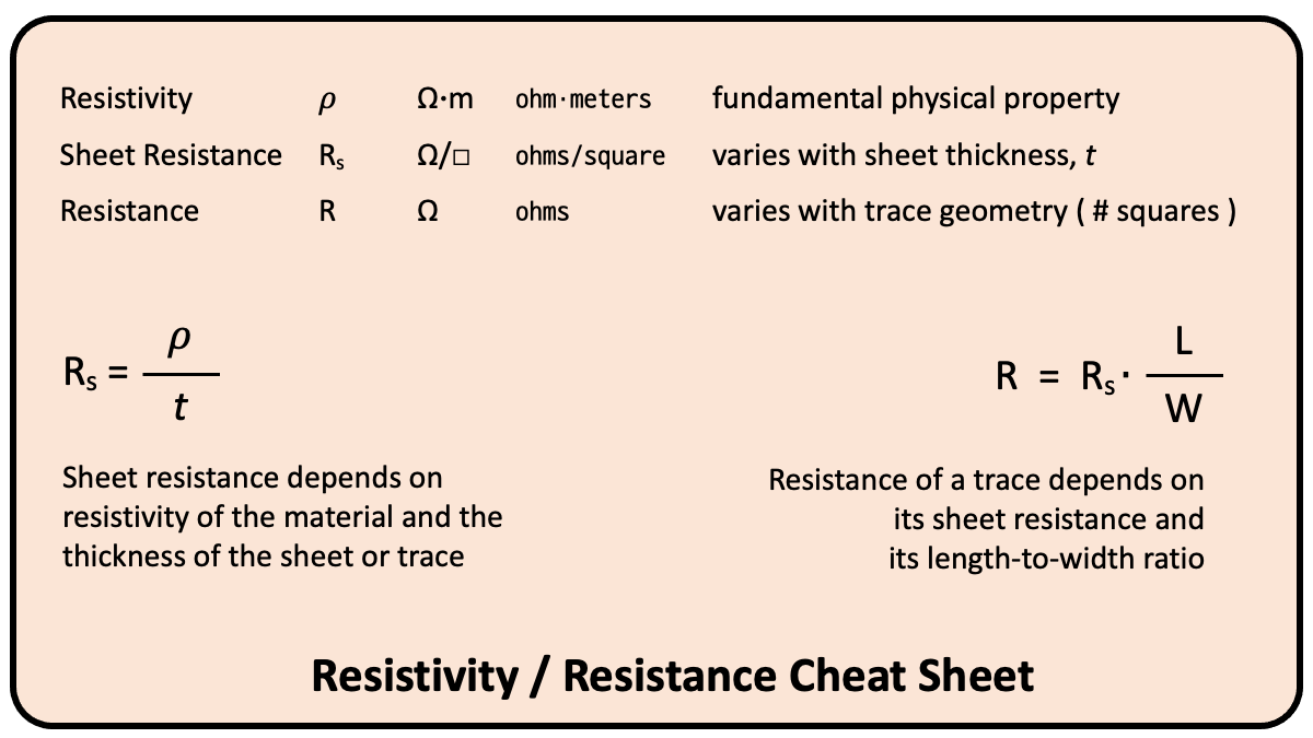
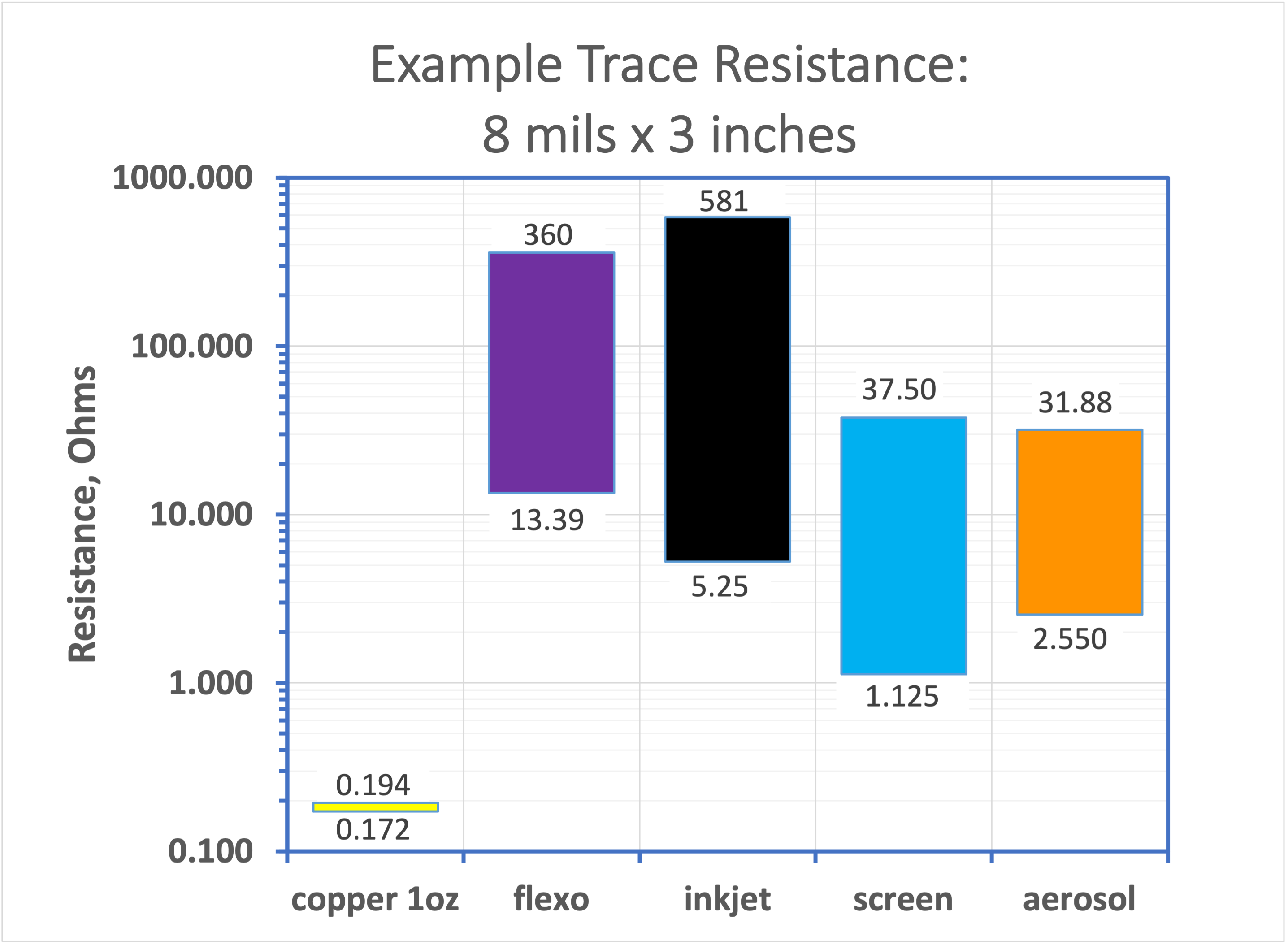
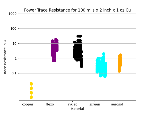
This figure shows trace resistances of typical PCB traces made from all different kinds of conductive inks. You can see the variety of resistances possible. Picking an ink for a particular project involves many other factors besides electrical properties. Cost, flexibility, substrate material, curing times and methods — the list goes on and on.
Takeaway
Lumped resistance, in the form of physical resistors, is a concept with which all electronics designers are familiar and comfortable. The physical property itself is bit peculiar, and one that isn’t normally thought about outside of niche applications. If you will be working with conductive ink printed circuit board designs, take some time to really get comfortable with the concepts in this article. Watch the video that I linked from Dave Jone’s EEVBlog channel on the subject. Search out other learning aids if necessary. If it helps, do some experiments yourself, either on the bench or simulated on the computer.
Theoretical Analyses
In parts 2 and 3 of the series, I made some calculations of what could be expected when using conductive inks in common electrical circuits. I optimistically concluded that the increased resistance of these traces should not pose any major problems for the vast majority of circuit classes. The most worrisome problem is of course distributing power. I speculated that making power traces much wider than normal should work in many applications.
For transient logic switching times, I performed a SPICE simulation and plotted the results at three different values of trace resistance. As expected, due to the interaction between the trace resistance and the input gate capacitance of typical ICs, the switching response time increased with increasing resistance:
- 5 ohms ~ 6 ns ~ 83.3 MHz
- 100 ohms ~ 27 ns ~ 18.5 MHz
- 500 ohms ~ 100 ns ~ 5.0 MHz
Takeaway
A wise boss and mentor taught me when I was a young engineer, before you embark on laboratory experiments you should have an idea of what to expect. This might not apply to people who make accidental discoveries, but for most of us, this is good advice to follow. Even if you can’t calculate the exact answer, at least knowing the bounds of your expected results can be helpful and save wasted time.
For this project, I analyzed the impact of having non-zero trace resistance for the kinds of circuits which appeared likely to be problematic. This isn’t perfect — the trace resistance could effect circuit types that my experience didn’t anticipate. Or perhaps second-order effects that I didn’t analyze could come into play. This doesn’t mean that advance analysis is useless, but be aware of these shortcomings if you observe unexpected results.
Building a Testing Environment
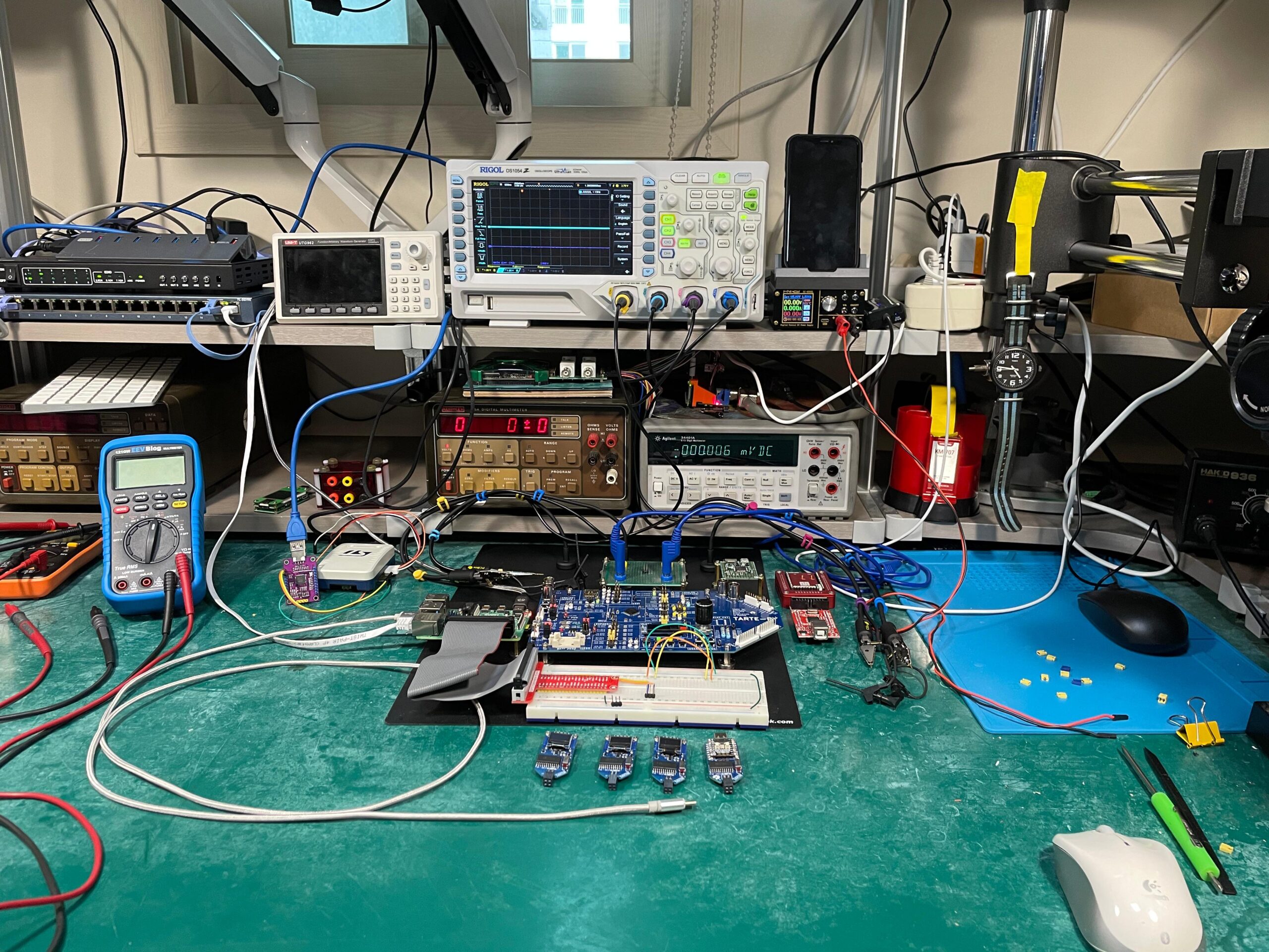
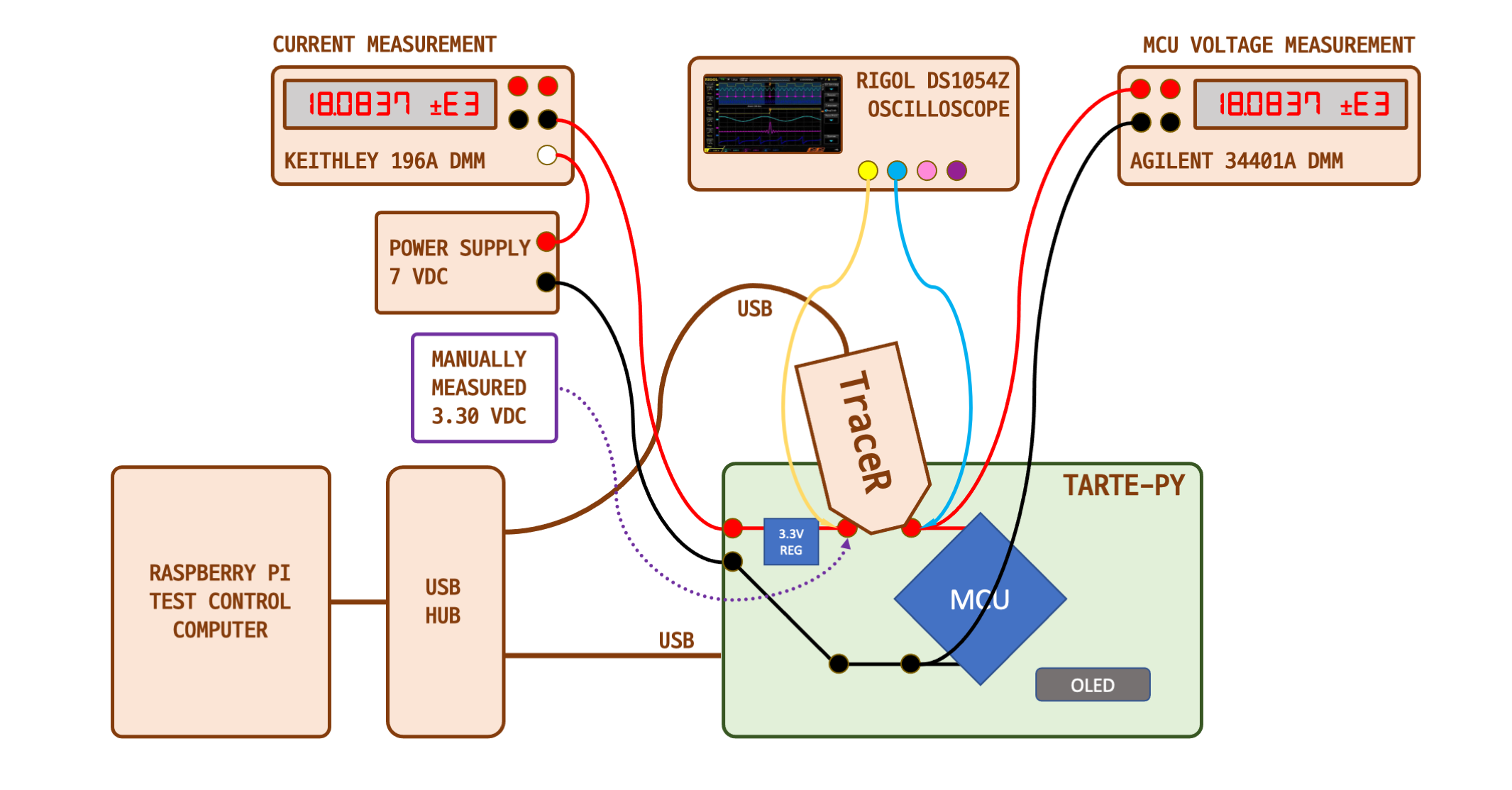
Parts 4 and 5 of the series were substantially dedicated to building and setting up a test bench. This allows us to experiment with different kinds of circuits while simulating arbitrary trace resistance. I designed a STM32F405 evaluation circuit board called the Tarte-Py. It is based on the reference Micropython Pyboard, but spread out to a much larger size so we can plug in simulated trace resistance modules. These modules also had to be designed and built, and I called them TraceR boards.
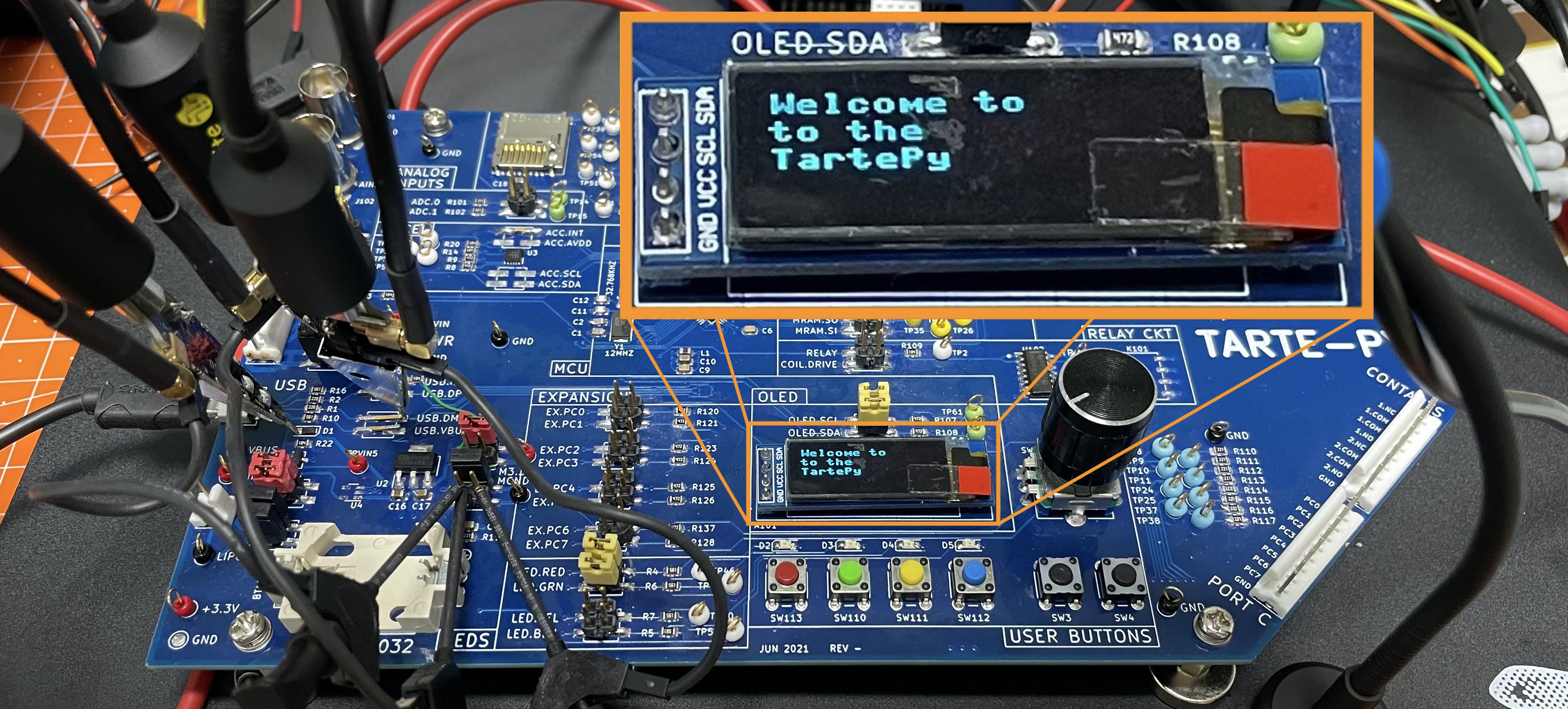
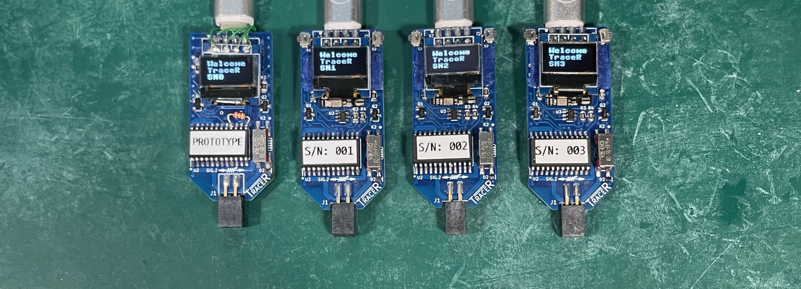
These custom boards, combined with a bunch of common laboratory test equipment and a Raspberry Pi test control computer make up our custom test bench.
Takeaway
Besides documenting the test environment for this series, I tried to show that you don’t have to break the bank to pull together a decent collection of quality test equipment. Older generation test gear can be very affordable. The majority of them are completely functional and, if needed, are still supported by professional calibration services. By using a scripting language like Python and the many supporting libraries, your can perform automated tests quite easily — something that’s typically been beyond the reach of for the hobbyist’s or small company’s electronic laboratories.
Experiment Results
I documented three basic experiments in parts 6 and 7, measuring serial link errors, MCU power failure, and high-speed rise times as a function of trace resistance. The results pretty much agreed with what we expected from the theory, which is always a good sign.
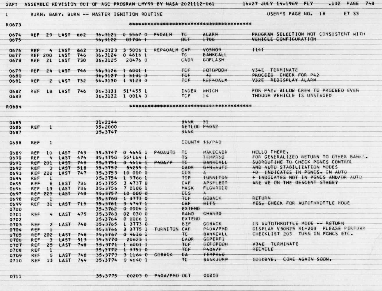
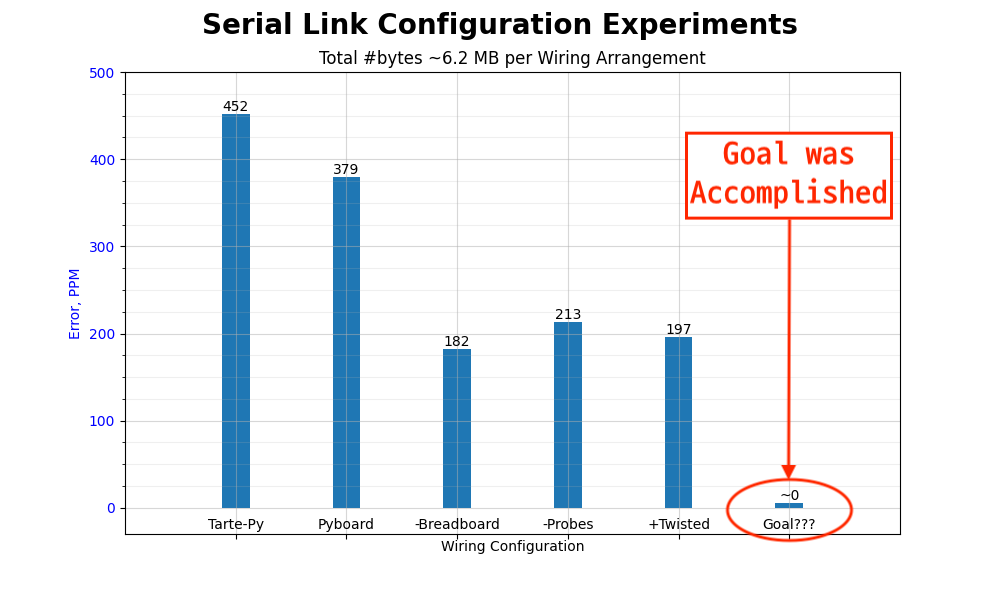
The complete source code from the Apollo 11 Lunar Lander computer was sent back and forth repeatedly over the serial link with different trace resistances. There was a small surprise when unexpected errors appeared in the serial link. This was eventually tracked down to a problem with the test rather than anything to do with trace resistance. Goal accomplished.
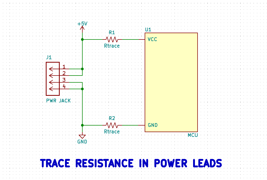
For the particular MCU on our Tarte-Py board, I found the maximum resistance that could be tolerated before the MCU died — 18.5 ohms. This is good news, when you compare it to the figure above showing the resistances of conductive ink power traces which are two inches long and 100 mils wide (that’s about 50 mm long by 2.5 mm wide). Such a trace made from any of the vast majority of inks will be well below this threshold.
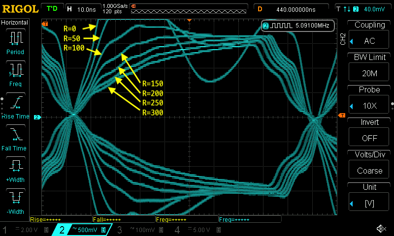
I plotted the eye diagram of a 5 MHz signal, showing the decrease in edge transition times vs increased trace resistance. The results are as expected, and we noted that designers of copper-traced-PCBs will often add resistors on such signals to slow down the rise times. This is done to decrease unintentional radiation from their circuits.
Takeaway
The observed results of these experiments were in general agreement with the analysis. And the issue of the unexpected serial link errors is a good example of why doing your analysis ahead of time can be helpful. When I started seeing these errors, I knew something was wrong based on my calculations and intuition. I just couldn’t believe that trace resistance was causing the errors. Further testing proved this was correct.
Advice for Designers
To summarize the lessons from this series, I can tabulate a few specific points.
- Keep trace lengths as short as possible
- High impedance circuits are less sensitive to trace resistance
- Many power supply connections will work if using extra-wide traces
- Put higher current drivers at the device they drive (e.g., relays and LEDs)
- Put lower impedance drivers at the edge of the design near their connectors
- Pay extra attention to:
- higher frequency signals
- signals requiring fast edge transitions
- Study carefully MCU operating voltage and current
Conclusion
What can we conclude, then, about circuits made from conductive inks? It’s difficult to generalize, since there are so many different applications. All the problems boil down to this point: even though copper isn’t a perfect conductor, in most designs we safely ignore its resistance. We can’t do that with conductive inks — we have to continually keep trace resistance in mind.
With a little extra planning and forethought, using conductive inks in your designs should not pose insurmountable problems. Just need to keep in mind the topics that were introduced in this series.
Future Articles
First of all, this test bench is now available for any further explorations which come to our attention. Feel free to let me know if you have any specific tests you’d like to see covered here.
I’ve been keeping a list of some detailed circuit ideas which could mitigate the non-zero resistances of conductive ink PCB traces. Among other one-part articles, I’m planning to start a new series on these mitigation techniques.

I am the proprietor of Chris’s Corner, an electrical engineer with more years in the field than I want to admit. I got hooked on electronics via Ham radio back in the 70s (WD4OLP / HL5ZJJ) and graduated from Georgia Tech in 1985. I’ve worked on all sorts of electronic projects, from government radars, NASA programs, industrial controllers, and consumer products. I’ve lived in South Korea for 20 years, where I’ve established a niche manufacturing company and an engineering consultancy. During pandemic I’ve sequestered myself here in my home office and laboratory, keeping busy on engineering projects and writing technical articles in my free time.

2 Responses
Hello,
I am a designer of disruptive technology specializing in printed conductive technology
and in particular the dissipation of warm air in the domestic home.
I would like to discuss with you, however, the patent office in the UK has strict rules
on disclosure prior to publication.
An NDA may be required.
Regards
Lawrence Karat
Hi Lawrence,
Feel free to contact me directly at stan.farnsworth@novacentrix.com and we’ll be glad to get the discussion started.
Best regards-
Stan