The performance demands of next-generation electronic systems—especially in biomedical devices, sensors, and RF platforms—are outpacing what traditional fabrication methods can deliver. Increasingly, designers require conductive materials that can support not only fine-line patterning but also vertically structured, high-aspect-ratio features on unconventional substrates. At NovaCentrix, we’ve developed advanced gold inks optimized for exactly these challenges, engineered for compatibility with high-resolution deposition systems like inkjet and aerosol jet printers.
Material Design for 3D and High-Fidelity Printing
NovaCentrix’s Metalon® gold inks are designed to meet the precision demands of modern additive electronics—particularly in biomedical engineering—where fine features, complex 3D geometries, and biocompatibility are all critical requirements. Two of our flagship inks, JG-125 and JG-024UA, exemplify this focus on performance and process adaptability.
JG-125 is a water-based gold nanoparticle ink optimized for inkjet printing, offering excellent stability, adhesion, and print fidelity on flexible and rigid substrates. It is well-suited for applications requiring fine-line patterning and high electrical conductivity, and can be processed with conventional thermal curing or advanced photonic techniques.
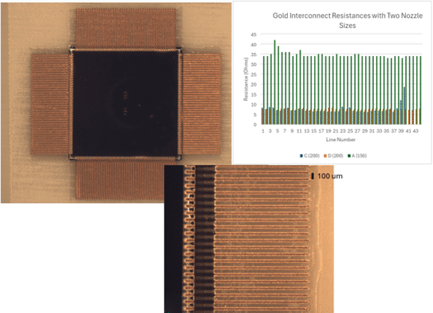
JG-024UA, on the other hand, is tailored for aerosol jet printing using ultrasonic atomization. With its higher solids content and carefully tuned rheology, this formulation supports the stable, high-resolution deposition needed for 3D microstructures, such as vertically printed micropillars and high-density interconnects.
In addition to their print fidelity and process compatibility, both JG-125 and JG-024UA deliver excellent electrical performance. When thermally cured, these inks achieve volume resistivities as low as 1.3 × 10⁻⁵ Ω-cm—less than 6X that of bulk gold. These inks can also be photonically-cured offering flexibility for temperature-sensitive substrates. This level of conductivity is critical for fine-feature and high-aspect-ratio designs where signal integrity, miniaturization, and reliability go hand in hand.
Together, these inks form a versatile platform for printed electronics—enabling both 2D and 3D additive manufacturing across biomedical, RF, and sensor applications, where precision, reliability, and biocompatibility are essential. In addition to our ink formulations, we also offer stable gold nanoparticle dispersions in water, available in concentrations ranging from 1% to 50% by weight. These are suitable for a variety of research applications beyond printed electronics.
Aerosol-Based Printing in Focus: Enabling High-Aspect-Ratio Microstructures


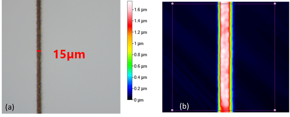
Aerosol jet printing (AJP) has emerged as a go-to technique for fine-line, high-aspect-ratio printing, especially when working with free-form or temperature-sensitive substrates. Our collaborations have allowed us to fine-tune ink formulations for our partners at IDS (JG-027UA-10%) and Optomec (JG-024UA), yielding compelling results in both resolution and z-axis structuring.
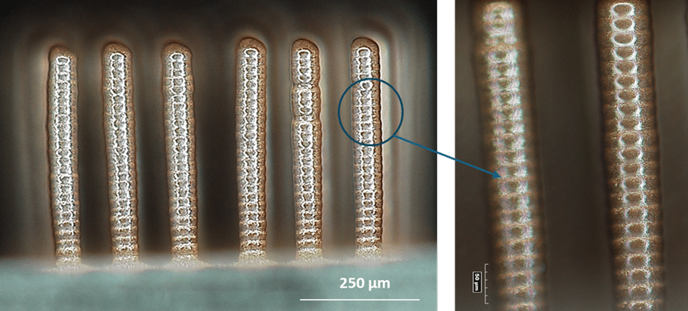
One of the most compelling demonstrations of this capability comes from KU Leuven, where researchers used a NovaCentrix-developed gold ink in a comprehensive design of experiments (DOE) study to fabricate arrays of 3D micropillars using ultrasonic-mode AJP on glass and flexible TPU films.
Using a 45 wt% AuNP-based ink (diluted 2:1 with MilliQ water for 3D builds), the team was able to:
- Print micropillar arrays as small as 50 µm in diameter
- Achieve heights up to 436 µm with an aspect ratio of 9.3
- Maintain shape fidelity using layer-by-layer builds in <10 minutes per structure
- Validate high electrical conductivity
- Demonstrate excellent biocompatibility with human fibroblast cell cultures
The optimized print condition delivered the best shape fidelity and vertical resolution with minimal overspray. Sintering at 200°C post-printing ensured dense and continuous conductive networks.

Proof-of-Concept: 3D Flexible Microelectrode Arrays
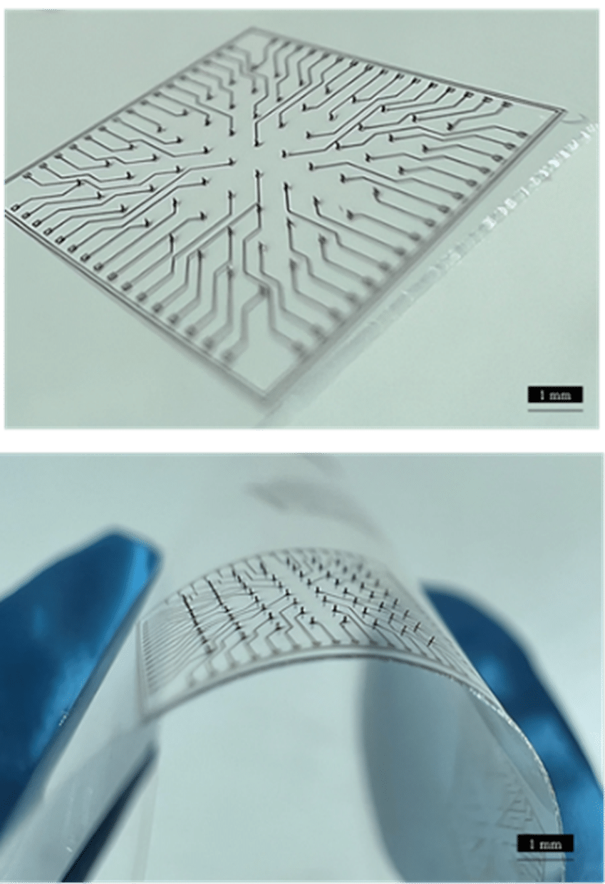
Taking this a step further, the team printed fully gold-based 3D MEA chips directly onto flexible TPU substrates. These devices, inspired by commercial 60MEA architectures, featured vertically printed micropillars on electrode pads with resolution down to 40 µm and a total device size under 12 mm. Notably, the devices retained their integrity and performance even under bending—highlighting the mechanical resilience of both the ink and the printing process.
This kind of structure—difficult or impossible to manufacture with conventional lithographic techniques—demonstrates the unique opportunity that additive manufacturing, combined with precision-engineered inks, brings to advanced electronics.

Broader Applications and Industry Validation
In addition to the KU Leuven work, NovaCentrix gold inks have been featured in several other high-impact 2024 studies, supporting applications such as:
- Flexible ceramic rectennas for wireless power (University of Washington)
- Organic electrochemical transistors (American University of Beirut and The University of Hong Kong)
- Thermoelectric generators (INRS-Canada)
- Biosensors for healthcare diagnostics (Old Dominion University)
Each of these examples underscores the versatility of our ink platform: printable on flexible substrates, compatible with sintering or photonic curing, and fine-tuned for mechanical, electrical, and biological integration.
Looking Ahead
The convergence of materials science and additive manufacturing is reshaping the future of electronics. By collaborating with researchers, equipment manufacturers, and device designers, NovaCentrix is helping to close the gap between materials capability and system-level need.
Our commitment is simple: to provide high-performance, application-driven ink solutions that unlock design freedom, miniaturization, and functional complexity—without compromising manufacturability or reliability.
If you have any specific conductive ink questions that need a customized materials solution we would love to chat. Please reach out at rudy.ghosh@novacentrix.com


