Photonic curing is the high temperature processing of thin films using a flashlamp. When this processing is performed on a low temperature substrate, such as plastic or paper, a significantly higher temperature can be attained in the film versus an oven without damaging the substrate. This is due to two effects: 1) thermal processes exponentially progress with increasing temperature and 2 ) thermal damage to a polymer substrate generally takes a finite amount of time. Within a range, the shorter the time, the higher the temperature a material can take without damage. In the case of a polymer or paper
substrate, the ultimate temperature one can reach is right below its gasification temperature. The result is that an intense pulse of light can process a thin absorbing film on a low temperature substrate in only a few hundred microseconds as effectively or better than 10 minutes in an oven. As the substrate generally absorbs less of the light energy from the flashlam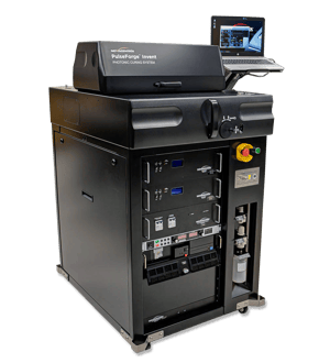 p than the targeted film, the film can be selectively printed and only the film is heated. That is, photonic curing is an automatically registering curing process. Consequently, even though photonic curing is very high in power, it is fundamentally a low energy process. Over the past 15 years, photonic curing has progressed far beyond the laboratory sintering of metal traces on plastic and paper and is now extensively used in many processes in the high-volume manufacturing (HVM) of consumer electronics.
It began with a $7 disposable camera
When we first developed the photonic curing process, the variables were not understood
particularly well. Our first demonstrator was performed with the flash unit from a $7
disposable camera! We had only a single control variable, and that was power. This
was controlled by varying the distance of the flash from the target. Still, we were able
to sinter dispersions of nanosilver as well as nanocopper particles on PET and paper to
form conductive traces almost instantly. The combination of high speed, large area, low
processing energy, plus coupled with automatic registration, meant it had the elements
of becoming an industrial process. All we had to do was scale it up.
As is often the case, the process of scale-up is where the real technology was developed. Flashlamps had been in existence for over 70 years. We had discovered a neat process and contacted established flashlamp manufacturers to build one for us. Unfortunately, there did not exist any commercial systems to perform this process at the industrial scale. Even rapid thermal processing (RTP) used in the semiconductor industry and intense pulsed light (IPL) used in the dermatology field, which are both flashlamp-based, were not high enough power or nearly at the scale we needed. So, we started building prototypes. Fortunately, we had some experience with pulsed power. We had previously worked on tokamaks and railguns, and early photonic curing systems were just scaled down versions of the 100,000 Amp pulsed arc discharge process we developed and used to make nanoparticles.
Still, building an industrial photonic curing tool was not just an issue of making a bigger beam, a larger power supply, and water cooling everything. We had to understand the process enough to control it.
Reinventing the flashlamp
Photonic curing is a thermal process, and on the most basic level, it has similarities with oven and laser processing. Yet, flashlamps generally have only limited use in industrial thermal processes. Traditionally, a flashlamp is driven by the discharge of a capacitor bank through an inductor in what is referred to as a pulse forming network (PFN). The purpose of the inductor is to slow down the rush of current from the capacitor bank. Changing the inductance value changes the characteristic “pulse length” of the discharge. In our early work, we suspected that the pulse length of the light from the flashlamp would affect this new process as our company had been varying the inductance of a 100,000 Amp PFN to control the average particle size in our nanoparticle synthesis process.
Our first prototype system had three different inductors, which meant three different pulse lengths. Whenever we wanted to change the pulse length, we had to power down the system, and change a busbar to reroute the current though a different inductor. Instead of being able to control just the voltage, which was related to instantaneous power, we could also change the pulse length too. Like a laser, the time integral over the whole pulse was related to the energy deposited per area. Like an oven, we were now up to two control variables: power and time. Our hypothesis was correct: Pulse length was important! Still, we realized that we needed to change the pulse length more quickly, and we wanted any pulse length, not just three values, as we were experimenting with many types of processes. This led to our first commercial photonic curing tool, the PulseForge 1100, which became commercially available in 2007. Using a more complex pulse forming network, this system allowed us to select any pulse length we desired. It was designed for R&D use, so the pulse rate repetition was only about 1 pulse every 10-20 seconds. The output was very high power though and allowed exploration of applications beyond sintering. It could even recrystallize amorphous silicon to form polycrystalline silicon!
We knew production applications would require very rapid pulse rates, plus the ability to synchronize the pulses to a moving sheet or a web of material. We envisioned curing printed electronics on plastic and paper as fast as it could be printed – just like a newspaper! This led to the development of the PulseForge 3100. Like the previous tool, it allowed us to select any voltage and pulse length we desired, but additionally allowed us to synchronize the pulse rate to the speed of a moving web and set the average number of pulses that the material received. Doing so allowed us to uniformly process kilometers of material in an R2R format. With the addition of those two more control variables, we were able to do some useful things that could not be done with an oven. For example, instead of pulsing our flashlamp at a constant rate, the pulse rate was synchronized with the web speed. That meant that we could get a uniform cure largely independent of the conveyance rate of the material being processed.
For the first time, the thermal processing rate on a web could be determined by limitations of other production steps instead of always being dominated by the large oven, which often took hours to heat up or cool down. Our 1-metre long tool could optimally process material even during ramp up and ramp down of the web speed. This resulted in less wasted material. Smaller footprint, less wasted material, and faster processing are attributes of photonic curing that continue to address pain points in materials thermal processing.
Going Digital
Advances continued, and we saw there was still more we could do. The use of variable inductance to control the pulse length was limiting us, and we already suspected that changing not only the length, but also the shape of the pulse was probably important. One can achieve almost any pulse shape with a complicated enough PFN, but changing the shape of the pulse using PFN methods is impractical. Consequently, we abandoned the PFN approach and updated the tools’ designs to utilize digital switching methods, capable of arbitrarily modulating the current to the lamp. This meant we were able to remove the inductor from our system entirely. Doing that allowed us to more rapidly cycle the flashlamp on and off, similar to pulse width modulation (PWM), to get any shaped pulse we desired. We called this pulse shaping. The adoption of the digital approach enabled over a dozen new machine variables for optimizing the process results.
In order to make sense of all the control parameters, we built a simulation for the output of the tool based on user-set control system parameters and embedded it into the tool’s control system. Since the temperature reached during photonic curing is dependent on the absorption of the materials being processed, the heat capacity, the thermal conductivity, and the thickness of each layer in the stack, we had to include provisions for those properties in the simulation. In order to make the process usable, we aggregated both the tool output simulation and the materials response simulation and integrated them into the tool.
Changing the settings on the machine actually ran the simulation, so the learning curve was very short, and the results were graphically displayed in less than a second. The output was a time-temperature history display of the thin film stack versus depth both during and after the exposure to the beam from the tool. We called this simulation aggregator SimPulse as it both simulated the dynamics of the pulse and made dealing with all the control variables simple.
Simple pulse vs shaped pulse
Two screen captures from the cloud version of SimPulse illustrate the heating profile for simple pulse (top image) versus shaped pulse (bottom image) photonic curing, respectively. In both cases, we have a simple two-layer stack comprising a 1-micron thick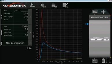 print of silver nanoparticle ink on top a 100-micron thick PET substrate. If this stack were oven cured, one would need to heat the entire stack up to about the 150°C temperature limit of PET and still require about 10 minutes to process the sample. Photonic curing can achieve a better cure, e.g. a higher electrical conductivity which is indicative of more complete sintering, with a single pulse of light. For the simple pulse case we emit about 0.7J/cm2 over 340 microseconds. Approximately 45% of the emission is absorbed by the ink and it is subsequently heated from 25°C to about 400°C. This is the approximate temperature limit one may reach when photonic curing on PET. After the beam is turned off, the thermal mass from the rest of the substrate rapidly cools the top of the substrate after processing. After about 20 milliseconds the entire stack reaches thermal equilibrium at about 55°C. The red trace shows the temperature over time at the top of the silver film. The yellow trace shows the temperature over time at the bottom of the PET substrate. Also note that there is no discernible temperature change at the bottom of the PET during processing. The blue trace shows the temperature over time at 10 microns below the silver film. Note that at no time does the substrate below the position graphed by blue line exceed 150°C during processing. Thus, the bulk of the substrate acts as a support for the portion which does exceed 150°C, and which would deform were it not for support from the underlying cooler material. In the simple pulse case, 400°C is only briefly reached.
With shaped pulse processing, we are able to slightly lower the maximum achieved temperature, to increase our processing margin, while staying at an overall elevated temperature point for much longer than in the simple pulse case. Like the simple pulse case, we initially pulse the flashlamp to heat the film to near 400°C. As the film begins to cool in about 50 microseconds, we give a smaller pulse of light to nudge the surface temperature back up. All the while, the heat from the top is being conducted into the bulk of the substrate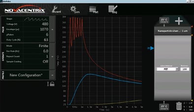 , so we continue to give small pulses to nudge the temperature back up again. The effect of this effort is that the amount of time spent just below the maximum allowed temperature is a lot longer than in the single pulse case. This results in a much better cure. In this example, we have used about 70% more radiant exposure, or a total of 1.2J/cm2. However, this is well below the damage threshold for PET. The final temperature after equilibration reaches about 80°C.
It is interesting to note that this simulation predicts that one may significantly reduce the thickness of the substrate, by about 2X, thereby saving money, without damaging the substrate. The simulation also predicts that with conductive cooling on the bottom of the substrate, one may reduce the thickness of the substrate by yet another factor of two!
Zone processing
What we have essentially accomplished with the shaped pulse photonic curing technique is the formation of a transient version of zone processing which is commonplace with industrial ovens. We ramp up, soak, and ramp down just as a zone processing oven does. Yet, this composite of pulses, or shaped pulse, is still completed on a timescale short enough to take advantage of the photonic curing effect, and that shaped pulse can still be repeated and synchronized to a moving web. The effect on curing is a dramatic improvement even over single pulse photonic curing.
In order to reliably perform shaped pulse processing, we first must have simulation of the tool output and the properties of the stack in order to know how to set the precise timing of the flashlamp pulses, as each pulse and delay is of a different duration. We also need to know what emission the machine is actually delivering. So, we use a bolometer developed in-house to directly measure the radiant exposure, measured in J/cm2, of each pulse. A bolometer has wonderful spectral response for our broadband beam, but sadly, it does not have the requisite megahertz data rate for continuous monitoring of the tool output. To augment the bolometer response, we also utilize an on-board, in-situ photodiode, which can be sampled at a megahertz rate. Measuring the pulse output with the bolometer, and then correlating that signal to the continuously-tracked photodiode data, forms a reliable, high-speed, and quantitative measurement of the light output from the tool. We are consequently able to place that data into a feedback loop to guarantee the tool has the same emission during long production runs. Similarly, we can use that feedback to adjust the tool conditions by electronically analyzing the cured material.
A few years ago, we had several models of photonic curing tools, but the demand for further customization began to increase. This resulted in the release of the PulseForge Invent (pictured above). The Invent is not a single machine configuration, but rather a highly customizable photonic curing R&D platform. As mentioned previously, our photonic curing simulation not only runs on every tool but over the cloud as well. This has the added benefit of enabling one to virtually configure a few dozen different tools and see the associated performance in each case. This technology saves customers a lot of money, as they don’t need to pay for functionality they don’t need, yet it still caters to what they do need.
It is accurate to say that we have a lot in common with LEGO building blocks in that we have modularized the functionality of our tools with well-designed components that stack together to give added functionality. The tools can be field-upgraded if needs change, aided with the same simulation. The transition from R&D to production uses yet again the same simulation to virtually build the production tool. Not only does that save time, but it also eliminates the cost and risk associated with scaleup. So, who would believe that 90 years after Harold “Doc” Edgerton invented the flashlamp, it is still advancing!